SNVSB57A October 2018 – May 2019 LMZM33604
PRODUCTION DATA.
- 1 Features
- 2 Applications
- 3 Description
- 4 Revision History
- 5 Pin Configuration and Functions
- 6 Specifications
-
7 Detailed Description
- 7.1 Overview
- 7.2 Functional Block Diagram
- 7.3
Feature Description
- 7.3.1 Adjusting the Output Voltage
- 7.3.2 Input Capacitor Selection
- 7.3.3 Output Capacitor Selection
- 7.3.4 Transient Response
- 7.3.5 Feed-Forward Capacitor
- 7.3.6 Switching Frequency (RT)
- 7.3.7 Synchronization (SYNC/MODE)
- 7.3.8 Output Enable (EN)
- 7.3.9 Programmable System UVLO (EN)
- 7.3.10 Internal LDO and BIAS_SEL
- 7.3.11 Power Good (PGOOD) and Power Good Pullup (PGOOD_PU)
- 7.3.12 Mode Select (Auto or FPWM)
- 7.3.13 Soft Start and Voltage Tracking
- 7.3.14 Voltage Dropout
- 7.3.15 Overcurrent Protection (OCP)
- 7.3.16 Thermal Shutdown
- 7.4 Device Functional Modes
- 8 Application and Implementation
- 9 Power Supply Recommendations
- 10Layout
- 11Device and Documentation Support
- 12Mechanical, Packaging, and Orderable Information
Package Options
Refer to the PDF data sheet for device specific package drawings
Mechanical Data (Package|Pins)
- RLX|41
Thermal pad, mechanical data (Package|Pins)
Orderable Information
7.3.1 Adjusting the Output Voltage
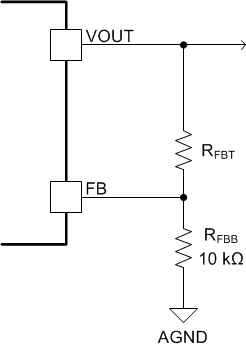
A resistor divider connected to the FB pin (pin 15) programs the output voltage of the LMZM33604. The output voltage adjustment range is from 1 V to 20 V. Figure 31 shows the feedback resistor connection for setting the output voltage. The recommended value of RFBB is 10 kΩ. The value for RFBT can be calculated using Equation 1.
Table 1 lists the standard external RFBT values for several standard output voltages along with the recommended switching frequency (FSW) and the frequency setting resistor (RRT) for each of the output voltages listed. (See Voltage Dropout for the allowable output voltage as a function of input voltage.)
space

where
- VFB (typical) = 1.006 V
 Figure 31. Setting the Output Voltage
 Table 1. Standard Component Values
| VOUT (V) | RFBT (kΩ)(1) | fSW (kHz) | RRT (kΩ) |
|---|---|---|---|
| 1.2 | 1.96 | 400 | 100 |
| 1.8 | 7.87 | 400 | 100 |
| 2.5 | 15.0 | 400 | 100 |
| 3.3 | 22.6 | 500 | 78.7 or open |
| 5 | 40.2 | 500 | 78.7 or open |
| 7.5 | 64.9 | 500 | 78.7 or open |
| 12 | 110 | 800 | 47.5 |
| 15 | 140 | 800 | 47.5 |
| 18 | 169 | 1000 | 38.3 |
| 20 | 191 | 1000 | 38.3 |