SNVSB11B June 2018 – May 2019 LMZM33606
PRODUCTION DATA.
- 1 Features
- 2 Applications
- 3 Description
- 4 Revision History
- 5 Pin Configuration and Functions
- 6 Specifications
-
7 Detailed Description
- 7.1 Overview
- 7.2 Functional Block Diagram
- 7.3
Feature Description
- 7.3.1 Adjusting the Output Voltage
- 7.3.2 Input Capacitor Selection
- 7.3.3 Output Capacitor Selection
- 7.3.4 Transient Response
- 7.3.5 Feed-Forward Capacitor
- 7.3.6 Switching Frequency (RT)
- 7.3.7 Synchronization (SYNC/MODE)
- 7.3.8 Output Enable (EN)
- 7.3.9 Programmable System UVLO (EN)
- 7.3.10 Internal LDO and BIAS_SEL
- 7.3.11 Power Good (PGOOD) and Power Good Pull-Up (PGOOD_PU)
- 7.3.12 Mode Select (Auto or FPWM)
- 7.3.13 Soft Start and Voltage Tracking
- 7.3.14 Voltage Dropout
- 7.3.15 Overcurrent Protection (OCP)
- 7.3.16 Thermal Shutdown
- 7.4 Device Functional Modes
- 8 Application and Implementation
- 9 Power Supply Recommendations
- 10Layout
- 11Device and Documentation Support
- 12Mechanical, Packaging, and Orderable Information
Package Options
Refer to the PDF data sheet for device specific package drawings
Mechanical Data (Package|Pins)
- RLX|41
Thermal pad, mechanical data (Package|Pins)
Orderable Information
10.3 Theta JA vs PCB Area
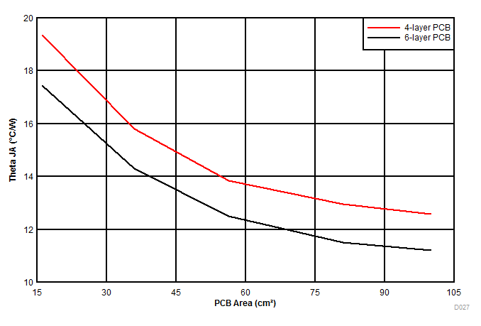
The amount of PCB copper effects the thermal performance of the device. Figure 52 shows the effects of copper area on the junction-to-ambient thermal resistance (RθJA) of the LMZM33606. The junction-to-ambient thermal resistance is plotted for a 4-layer PCB and a 6-layer PCB with PCB area from 16 cm2 to 100 cm2.
To determine the required copper area for an application:
- Determine the maximum power dissipation of the device in the application by referencing the power dissipation graphs in the Typical Characteristics section.
- Calculate the maximum θJA using Equation 8 and the maximum ambient temperature of the application.
- Reference Figure 52 to determine the minimum required PCB area for the application conditions.
Equation 8. 

 Figure 52. θJA vs PCB Area