SNVSB11B June   2018  – May 2019 LMZM33606

PRODUCTION DATA.  

  1. Features
  2. Applications
    1.     Simplified Schematic
  3. Description
    1.     Minimum Solution Size
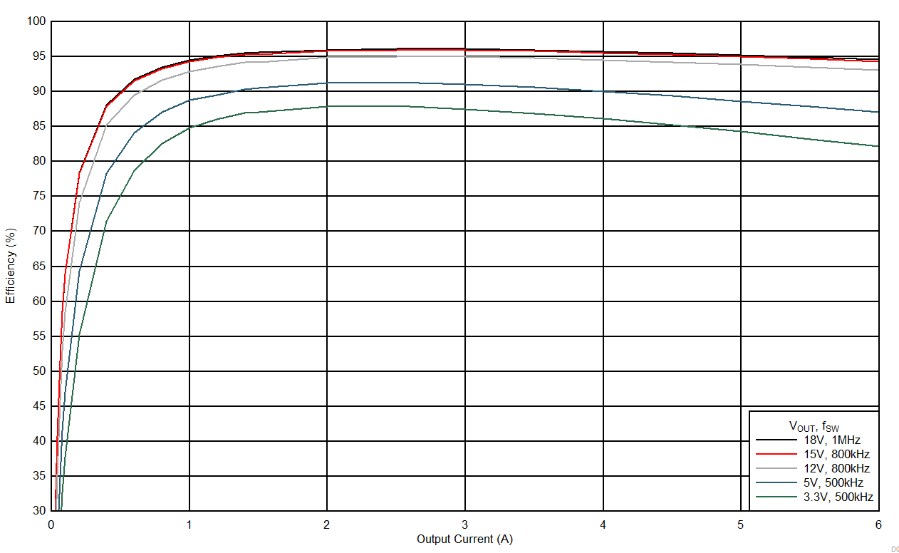
    2.     Typical Efficiency (Auto Mode)
  4. Revision History
  5. Pin Configuration and Functions
    1.     Pin Functions
  6. Specifications
    1. 6.1 Absolute Maximum Ratings
    2. 6.2 ESD Ratings
    3. 6.3 Recommended Operating Conditions
    4. 6.4 Thermal Information
    5. 6.5 Electrical Characteristics
    6. 6.6 Switching Characteristics
    7. 6.7 Typical Characteristics (VIN = 12 V)
    8. 6.8 Typical Characteristics (VIN = 24 V)
    9. 6.9 Typical Characteristics (VIN = 36 V)
  7. Detailed Description
    1. 7.1 Overview
    2. 7.2 Functional Block Diagram
    3. 7.3 Feature Description
      1. 7.3.1  Adjusting the Output Voltage
      2. 7.3.2  Input Capacitor Selection
      3. 7.3.3  Output Capacitor Selection
      4. 7.3.4  Transient Response
      5. 7.3.5  Feed-Forward Capacitor
      6. 7.3.6  Switching Frequency (RT)
      7. 7.3.7  Synchronization (SYNC/MODE)
      8. 7.3.8  Output Enable (EN)
      9. 7.3.9  Programmable System UVLO (EN)
      10. 7.3.10 Internal LDO and BIAS_SEL
      11. 7.3.11 Power Good (PGOOD) and Power Good Pull-Up (PGOOD_PU)
      12. 7.3.12 Mode Select (Auto or FPWM)
      13. 7.3.13 Soft Start and Voltage Tracking
      14. 7.3.14 Voltage Dropout
      15. 7.3.15 Overcurrent Protection (OCP)
      16. 7.3.16 Thermal Shutdown
    4. 7.4 Device Functional Modes
      1. 7.4.1 Active Mode
      2. 7.4.2 Auto Mode
      3. 7.4.3 FPWM Mode
      4. 7.4.4 Shutdown Mode
  8. Application and Implementation
    1. 8.1 Application Information
    2. 8.2 Typical Application
      1. 8.2.1 Design Requirements
      2. 8.2.2 Detailed Design Procedure
        1. 8.2.2.1 Output Voltage Setpoint
        2. 8.2.2.2 Setting the Switching Frequency
        3. 8.2.2.3 Input Capacitors
        4. 8.2.2.4 Output Capacitor Selection
        5. 8.2.2.5 Feed-Forward Capacitor (CFF)
        6. 8.2.2.6 Application Curves
  9. Power Supply Recommendations
  10. 10Layout
    1. 10.1 Layout Guidelines
    2. 10.2 Layout Example
    3. 10.3 Theta JA vs PCB Area
    4. 10.4 Package Specifications
    5. 10.5 EMI
      1. 10.5.1 EMI Plots
  11. 11Device and Documentation Support
    1. 11.1 Device Support
      1. 11.1.1 Third-Party Products Disclaimer
    2. 11.2 Receiving Notification of Documentation Updates
    3. 11.3 Community Resources
    4. 11.4 Trademarks
    5. 11.5 Electrostatic Discharge Caution
    6. 11.6 Glossary
  12. 12Mechanical, Packaging, and Orderable Information
    1. 12.1 Tape and Reel Information

Package Options

Refer to the PDF data sheet for device specific package drawings

Mechanical Data (Package|Pins)
  • RLX|41
Thermal pad, mechanical data (Package|Pins)
Orderable Information

Typical Characteristics (VIN = 24 V)

The typical characteristic data has been developed from actual products tested at 25°C. This data is considered typical for the device.
LMZM33606 D004_24VeffPWMLin2.gif
FPWM Mode Linear Scale
Figure 11. Efficiency vs Output Current
LMZM33606 D005_24VeffPWMLog.gif
FPWM Mode Log Scale
Figure 13. Efficiency vs Output Current
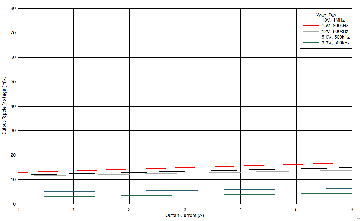
LMZM33606 D007_24VRippleFPWM1.gif
FPWM Mode COUT = 4 × 47 µF ceramic
Figure 15. Output Voltage Ripple
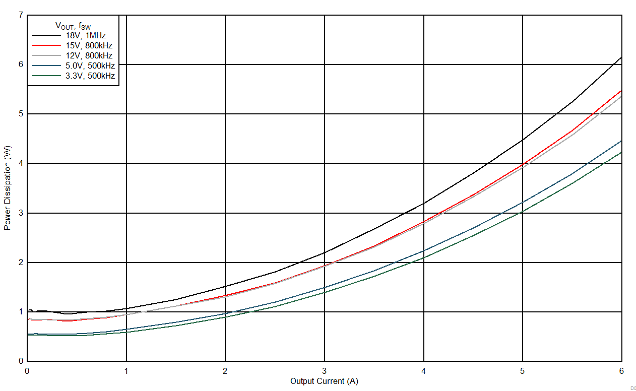
LMZM33606 D008_24VPdis.gif
Figure 17. Power Dissipation
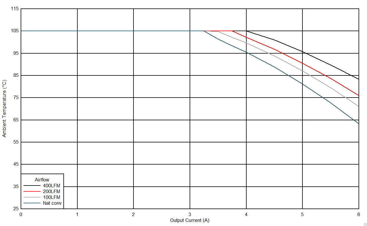
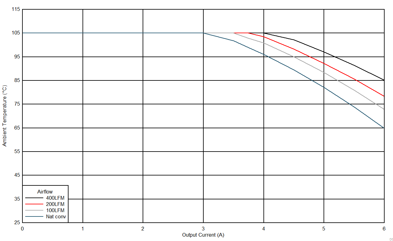
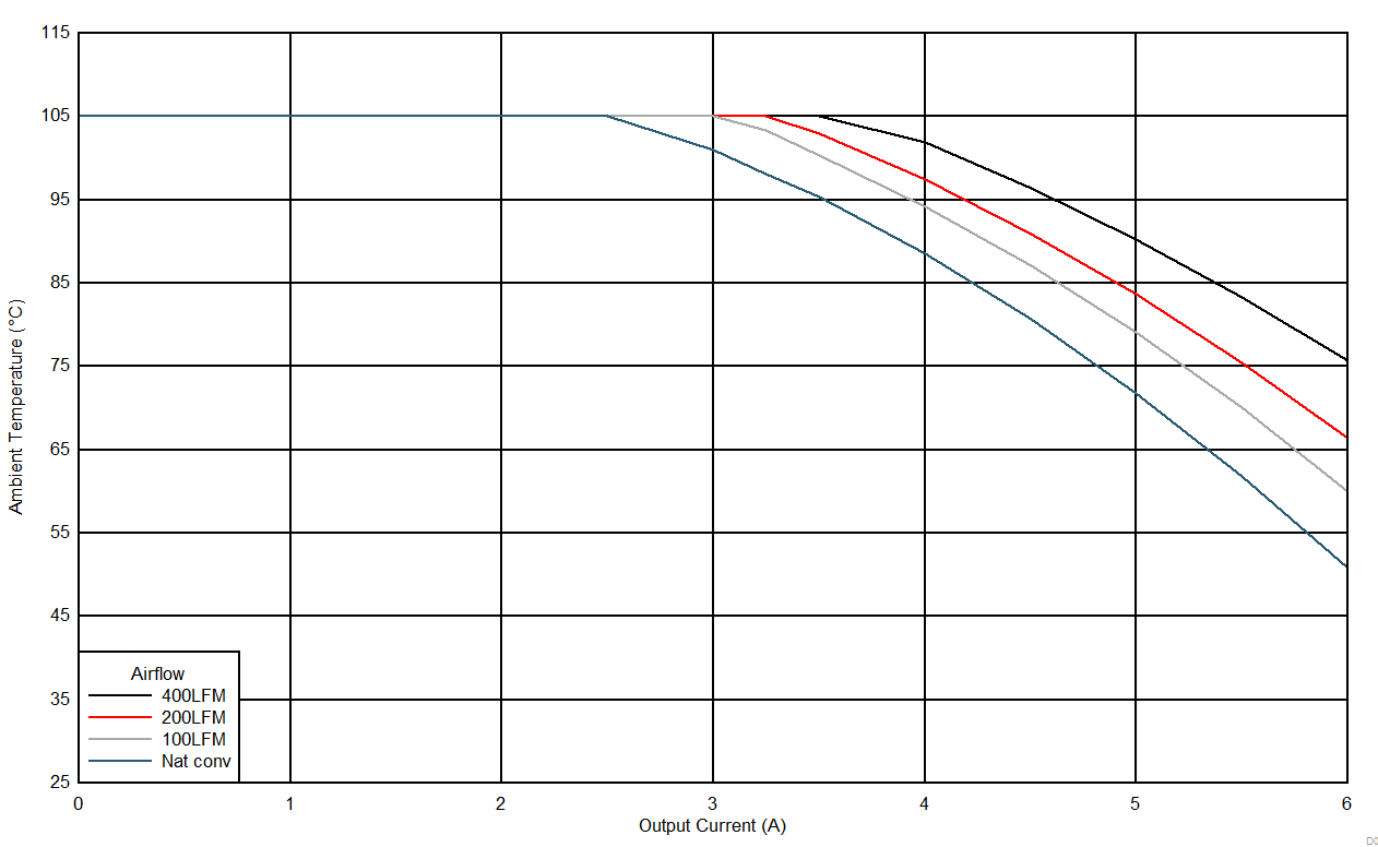
LMZM33606 D010_24Vto5VSOA.gif
VOUT = 5 V fSW = 500 kHz
PCB = 75 mm × 75 mm, 4-layer, 2 oz. copper
Figure 19. Safe Operating Area
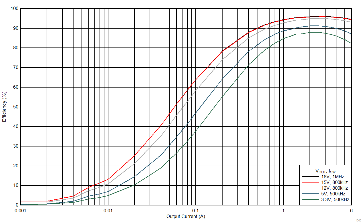
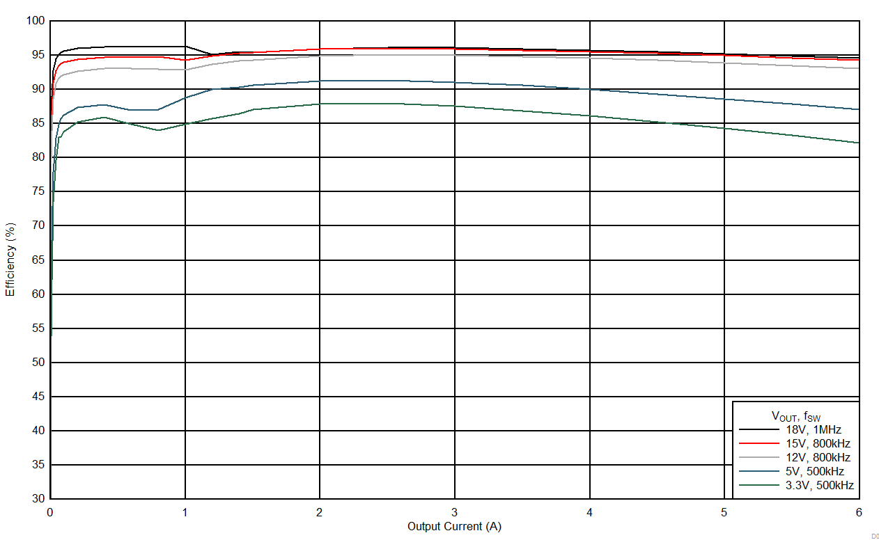
LMZM33606 D002_24VeffAutoLin2.gif
Auto Mode Linear Scale
Figure 12. Efficiency vs Output Current
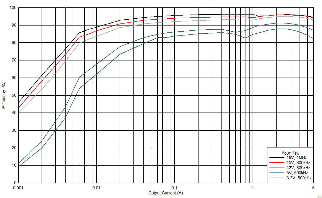
LMZM33606 D003_24VeffAutoLog.gif
Auto Mode Log Scale
Figure 14. Efficiency vs Output Current
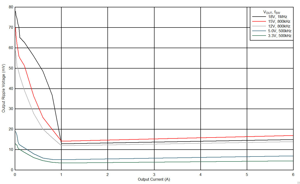
LMZM33606 D006_24VRippleAuto.gif
Auto Mode COUT = 4 × 47 µF ceramic
Figure 16. Output Voltage Ripple
LMZM33606 D011_24Vto33VSOA.gif
VOUT = 3.3 V fSW = 500 kHz
PCB = 75 mm × 75 mm, 4-layer, 2 oz. copper
Figure 18. Safe Operating Area
LMZM33606 D009_24Vto12VSOA.gif
VOUT = 12 V fSW = 800 kHz
PCB = 75 mm × 75 mm, 4-layer, 2 oz. copper
Figure 20. Safe Operating Area