SNVS764Q January 2000 – December 2017 LP2950-N , LP2951-N
PRODUCTION DATA.
- 1 Features
- 2 Applications
- 3 Description
- 4 Revision History
- 5 Voltage Options
- 6 Pin Configuration and Functions
- 7 Specifications
-
8 Detailed Description
- 8.1 Overview
- 8.2 Functional Block Diagrams
- 8.3 Feature Description
- 8.4 Device Functional Modes
-
9 Application and Implementation
- 9.1 Application Information
- 9.2
Typical Applications
- 9.2.1 1-A Regulator with 1.2-V Dropout
- 9.2.2 300-mA Regulator with 0.75-V Dropout
- 9.2.3 Wide Input Voltage Range Current Limiter
- 9.2.4 Low Drift Current Source
- 9.2.5 5-V Current Limiter
- 9.2.6 Regulator with Early Warning and Auxiliary Output
- 9.2.7 Latch Off When Error Flag Occurs
- 9.2.8 2-A Low Dropout Regulator
- 9.2.9 5-V Regulator with 2.5-V Sleep Function
- 9.2.10 Open Circuit Detector for 4 → 20-mA Current Loop
- 9.2.11 Regulator with State-of-Charge Indicator
- 9.2.12 Low Battery Disconnect
- 9.2.13 System Overtemperature Protection Circuit
- 10Power Supply Recommendations
- 11Layout
- 12Device and Documentation Support
- 13Mechanical, Packaging, and Orderable Information
Package Options
Mechanical Data (Package|Pins)
Thermal pad, mechanical data (Package|Pins)
Orderable Information
9 Application and Implementation
NOTE
Information in the following applications sections is not part of the TI component specification, and TI does not warrant its accuracy or completeness. TI’s customers are responsible for determining suitability of components for their purposes. Customers should validate and test their design implementation to confirm system functionality.
9.1 Application Information
The LP2950-N and LP2951-N are linear voltage regulator operating from 2.3 V to 30 V on the input and regulates voltages between 1.24 V to 29 V with 0.5% accuracy and 160 mA maximum outputs current. Efficiency is defined by the ratio of output voltage to input voltage because the LP2950-N and LP2951-N is a linear voltage regulator. To achieve high efficiency, the dropout voltage (VIN – VOUT) must be as small as possible, thus requiring a very low dropout LDO. Successfully implementing an LDO in an application depends on the application requirements. If the requirements are simply input voltage and output voltage, compliance specifications (such as internal power dissipation or stability) must be verified to ensure a solid design. If timing, start-up, noise, PSRR, or any other transient specification is required, the design becomes more challenging.
 Figure 35. Schematic Diagram
9.2 Typical Applications
9.2.1 1-A Regulator with 1.2-V Dropout
 Figure 36. 1-A Regulator with 1.2-V Dropout
9.2.1.1 Design Requirements
For this design example, use the parameters listed in Table 1 as the input parameters.
Table 1. Design Parameters
| DESIGN PARAMETER | DESIGN REQUIREMENT |
|---|---|
| Input voltage | 6.5 V, ±10%, provided by the DC-DC converter switching at 1 MHz |
| Output voltage | 5 V, ±1% |
| Output current | 100 mA (maximum), 1 mA (minimum) |
| RMS noise, 10 Hz to 100 kHz | < 200 µVRMS |
| PSRR at 1 KHz | > 50 dB |
9.2.1.2 Detailed Design Procedure
At 100-mA loading, the dropout of the LP2950-N/LP2951-N has 600 mV maximum dropout over temperature, thus an 1500-mV headroom is sufficient for operation over both input and output voltage accuracy. The efficiency of the LP2950-N/LP2951-N in this configuration is VOUT / VIN = 76.9%. To achieve the smallest form factor, the TO-92 package is selected. Input and output capacitors are selected in accordance with the Capacitor Recommendation section. Ceramic capacitances of 1 µF for the input and one 2.2-µF capacitors for the output are selected. With an efficiency of 73.3% and a 100-mA maximum load, the internal power dissipation is 150 mW, which corresponds to a 18.9°C junction temperature rise for the TO-92 package. With an 85°C maximum ambient temperature, the junction temperature is at 103.9°C. To minimize noise, a bypass capacitance (CBYPASS) of 0.01-µF is selected between pin 7 to pin 1 for LP2951-N.
9.2.1.2.1 Output Capacitor Requirements
A 1-µF (or greater) capacitor is required between the output and ground for stability at output voltages of 5 V or higher. At lower output voltages, more capacitance is required (2.2 µF or more is recommended for 3-V and
3.3-V versions). Without this capacitor the device oscillates. Most types of tantalum or aluminum electrolytic work fine here; even film types work but are not recommended for reasons of cost. Many aluminum electrolytics have electrolytes that freeze at about −30°C, so solid tantalums are recommended for operation below −25°C. The important parameters of the capacitor are an ESR of about 5 Ω or less and a resonant frequency above 500 kHz. The value of this capacitor may be increased without limit.
 Figure 37. Output Capacitor ESR Range
The reason for the lower ESR limit is that the loop compensation of the feedback loop relies on the capacitance value and the ESR value of the output capacitor to provide the zero that gives added phase lead (See Figure 37).
Using the 2.2 µF value from the Output Capacitor ESR Range curve (Figure 37), a useful range for fZ can be estimated:
For ceramic capacitors, the low ESR produces a zero at a frequency that is too high to be useful, so meaningful phase lead does not occur. A ceramic output capacitor can be used if a series resistance is added (recommended value of resistance about 0.1 Ω to 2 Ω) to simulate the needed ESR. Only X5R, X7R, or better, MLCC types should be used, and should have a DC voltage rating at least twice the VOUT(NOM) value.
At lower values of output current, less output capacitance is required for stability. The capacitor can be reduced to 0.33 µF for currents below 10 mA or 0.1 µF for currents below 1 mA. Using the adjustable versions at voltages below 5 V runs the error amplifier at lower gains so that more output capacitance is needed. For the worst-case situation of a 100-mA load at 1.23 V output (output shorted to Feedback) a 3.3-µF (or greater) capacitor should be used.
Unlike many other regulators, the LP2950-N remains stable and in regulation with no load in addition to the internal voltage divider. This is especially important in CMOS RAM keep-alive applications. When setting the output voltage of the LP2951-N versions with external resistors, a minimum load of 1 µA is recommended.
Applications having conditions that may drive the LP2950-N/51 into nonlinear operation require special consideration. Nonlinear operation occurs when the output voltage is held low enough to force the output stage into output current limiting while trying to pull the output voltage up to the regulated value. The internal loop response time controls how long it takes for the device to regain linear operation when the output has returned to the normal operating range. There are three significant nonlinear conditions that need to be considered, all can force the output stage into output current limiting mode, all can cause the output voltage to over-shoot with low value output capacitors when the condition is removed, and the recommended generic solution is to set the output capacitor to a value not less than 10 µF. Although the 10 µF value for COUT may not eliminate the output voltage over-shoot in all cases, it should lower it to acceptable levels (< 10% of VOUT(NOM)) in the majority of cases. In all three of these conditions, applications with lighter load currents are more susceptible to output voltage over-shoot than applications with higher load currents.
- At power-up, with the input voltage rising faster than output stage can charge the output capacitor.
- ΔVIN = VOUT(NOM) + 1 V
- Recovery from an output short circuit to ground condition.
- Toggling the LP2951-N SHUTDOWN pin from high (OFF) to low (ON).
where
 Figure 38. LP2951-N Enable Transient
9.2.1.2.2 Input Capacitor Requirements
A minimum 1 µF tantalum, ceramic or aluminum electrolytic capacitor should be placed from the LP2950-N/LP2951-N input pin to ground if there is more than 10 inches of wire between the input and the AC filter capacitor or if a battery is used as the input.
9.2.1.2.3 Error Detection Comparator Output
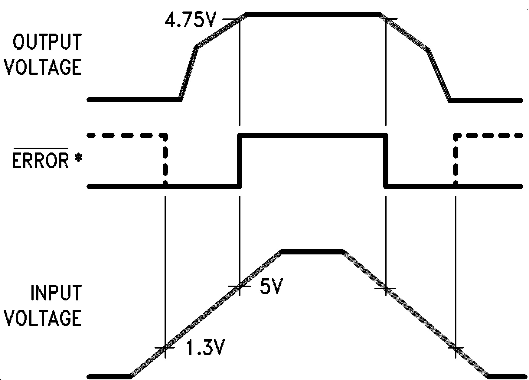
The comparator produces a logic low output whenever the LP2951-N output falls out of regulation by more than approximately 5%. This figure is the comparator's built-in offset of about 60 mV divided by the 1.235 reference voltage. (Refer to the block diagram in the front of the datasheet.) This trip level remains “5% below normal” regardless of the programmed output voltage of the 2951. For example, the error flag trip level is typically 4.75 V for a 5-V output or 11.4 V for a 12-V output. The out of regulation condition may be due either to low input voltage, current limiting, or thermal limiting.
Figure 39 below gives a timing diagram depicting the ERROR signal and the regulated output voltage as the LP2951-N input is ramped up and down. For 5 V versions, the ERROR signal becomes valid (low) at about 1.3-V input. It goes high at about 5-V input (the input voltage at which VOUT = 4.75 V). Because the LP2951-N dropout voltage is load-dependent (see curve in typical performance characteristics), the input voltage trip point (about 5 V) varies with the load current. The output voltage trip point (approx. 4.75 V) does not vary with load.
The error comparator has an open-collector output which requires an external pull up resistor. This resistor may be returned to the output or some other supply voltage depending on system requirements. In determining a value for this resistor, note that while the output is rated to sink 400 µA, this sink current adds to battery drain in a low battery condition. Suggested values range from 100 k to 1 MΩ. The resistor is not required if this output is unused.
9.2.1.2.4 Programming the Output Voltage (LP2951-N)
The LP2951-N may be pin-strapped for the nominal fixed output voltage using its internal voltage divider by tying the output and sense pins together, and also tying the FEEDBACK and VTAP pins together. Alternatively, it may be programmed for any output voltage between its 1.235-V reference and its 30-V maximum rating. As seen in Figure 40, an external pair of resistors is required.
The complete equation for the output voltage is

where
- VREF is the nominal 1.235-V reference voltage and IFB is the FEEDBACK pin bias current, nominally –20 nA
The minimum recommended load current of 1 µA forces an upper limit of 1.2 MΩ on the value of R2, if the regulator must work with no load (a condition often found in CMOS in standby). IFB produces a 2% typical error in VOUT which may be eliminated at room temperature by trimming R1. For better accuracy, choosing R2 = 100 kΩ reduces this error to 0.17% while increasing the resistor program current to 12 µA. Because the LP2951-N typically draws 60 µA at no load with pin 2 open-circuited, this is a small price to pay.


*Drive with TTL-high to shut down. Ground or leave open if shutdown feature is not to be used.
Note: Pins 2 and 6 are left open.
Stray capacitance to the LP2951-N FEEDBACK pin can cause instability. This may especially be a problem when using high value external resistors to set the output voltage. Adding a 100-pF capacitor between the OUT pin and the FEEDBACK pin, and increasing the output capacitor to at least 3.3 µF, fixes this problem.
9.2.1.2.5 Reducing Output Noise
In reference applications it may be advantageous to reduce the AC noise present at the output. One method is to reduce the regulator bandwidth by increasing the size of the output capacitor. This is the only way noise can be reduced on the 3-lead LP2950-N but is relatively inefficient, as increasing the capacitor from 1 µF to 220 µF only decreases the noise from 430 µVRMS to 160 µVRMS for a 100-kHz bandwidth at 5-V output.
Noise can be reduced fourfold by a bypass capacitor across R1, because it reduces the high frequency gain from 4 to unity. Pick

or about 0.01 µF. When doing this, the output capacitor must be increased to 3.3 µF to maintain stability. These changes reduce the output noise from 430 µV to 100 µV rms for a 100-kHz bandwidth at 5-V output. With the bypass capacitor added, noise no longer scales with output voltage so that improvements are more dramatic at higher output voltages.
9.2.1.3 Application Curves
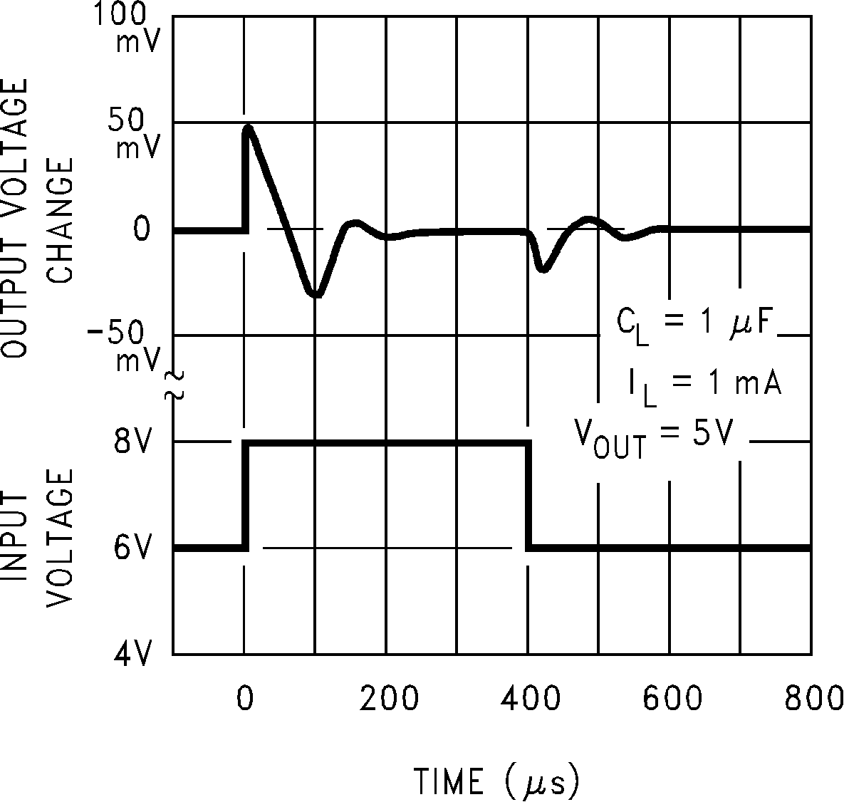 Figure 41. Line Transient Response
 Figure 43. Load Transient Response
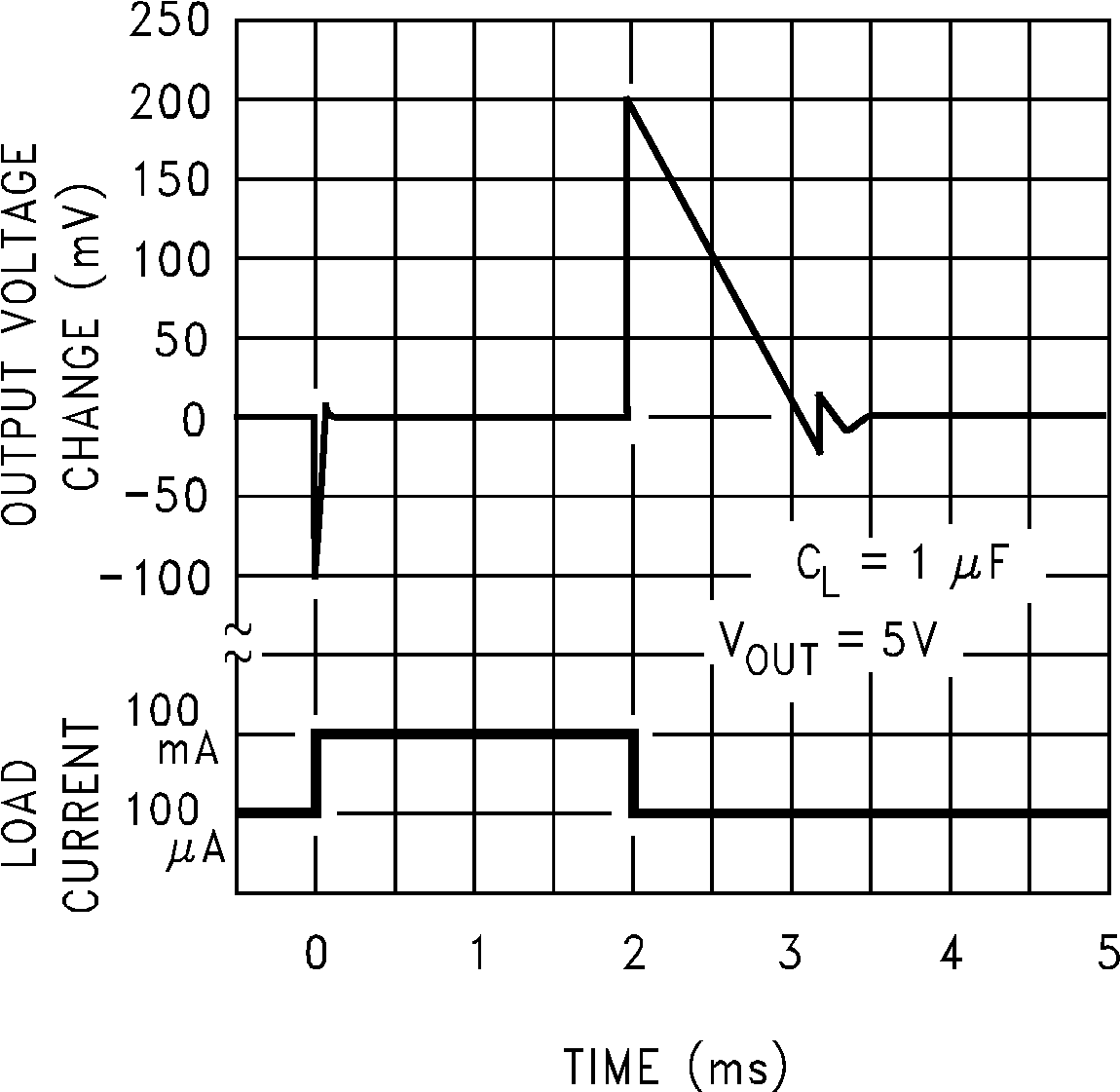 Figure 42. Load Transient Response
9.2.2 300-mA Regulator with 0.75-V Dropout
In Figure 44, by paralleling the LP2951 together with 2x2N5432 (150-mA N channel JFET), a user can get a higher output current capability around 300 mA.
 Figure 44. 300-mA Regulator with 0.75-V Dropout
9.2.3 Wide Input Voltage Range Current Limiter
The LP2951 can be used as a 160-mA current limiter as Figure 45. When FB is connected to ground, the pass element is fully turned on and out voltage will be close to input voltage. Input-output voltage ranges from 40 mV to 400 mV, depending on load current.

9.2.4 Low Drift Current Source
The LP2951 can be used as a low drift current source as Figure 46 shows. By connected Vout to FB, Vout will regulated at 1.235 V, and current consumption at R is IL = 1.23/R.
 Figure 46. Low Drift Current Source
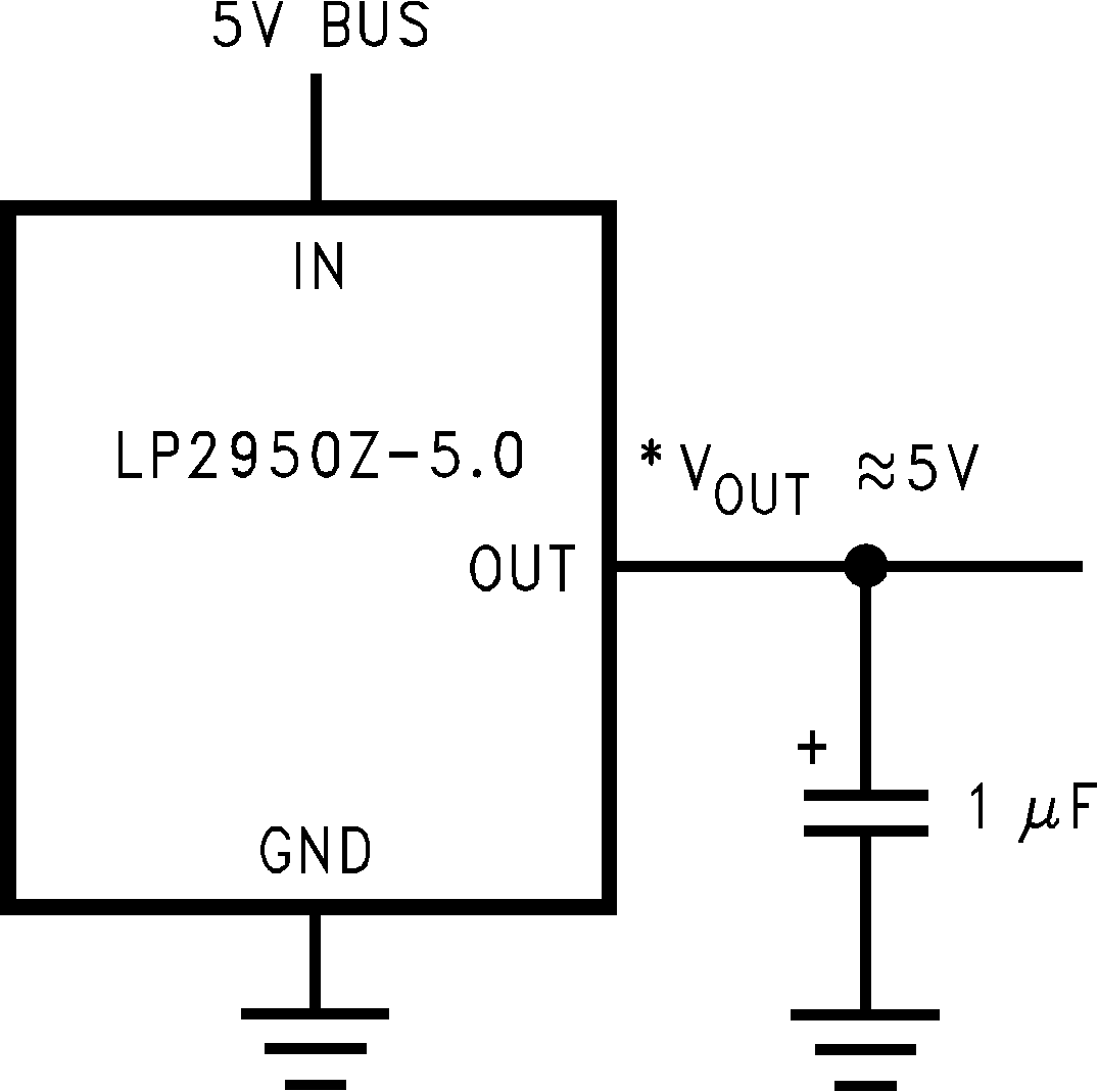
9.2.5 5-V Current Limiter
The LP2950 internal current limit function can be leveraged to build 5-V current limiter as Figure 47 shows. The minimum input-output voltage ranges from 40 mV to 400 mV, depending on load current. Current limit is typically 160 mA.
9.2.6 Regulator with Early Warning and Auxiliary Output
The LP2951 can be used to build a Regulator with early warning and auxiliary output as Figure 48 shows. it has below features:
- Early warning flag on low input voltage
- Main output latches off at lower input voltages
- Battery backup on auxiliary output
- Operation: VOUT of regulator 1 is programmed one diode drop above 5 V. Its error flag becomes active when VIN ≤ 5.7 V. When VIN drops below 5.3 V, the error flag of regulator 2 becomes active and via Q1 latches the main output off. When VIN again exceeds 5.7 V regulator 1 is back in regulation and the early warning signal rises, unlatching regulator 2 via D3.
 Figure 48. Regulator With Early Warning and Auxiliary Output
9.2.7 Latch Off When Error Flag Occurs
As Figure 49 presents, a latch off when error flag occurs circuit works in below two mode:
When output is within ±95% of VOUT option, the error flag pin keep output high, which turns off PNP bipolar and pulls SD pin to low, then the LP2951 keeps output regulated voltage.
When output drop to less than 95% of VOUT option, it triggers error flag output a low voltage, which turns on PNP bipolar and pulls SD pin to high, then the device enters shutdown mode and turns off output voltage. During a shutdown sequence, the ERROR pin continues output low, and the LP2951 device latches in shutdown mode.
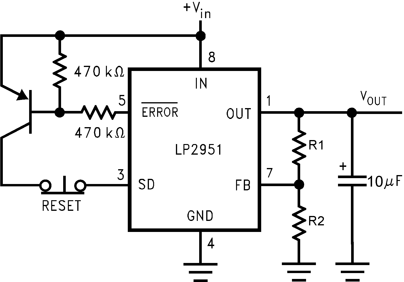 Figure 49. Latch Off When Error Flag Occurs
9.2.8 2-A Low Dropout Regulator
As Figure 50 shows, the 2-A low dropout regulator has below features:

For 5 VOUT, use internal resistors. Wire pin 6 to pin 7 and wire pin 2 to + VOUT bus.
 Figure 50. 2-A Low Dropout Regulator
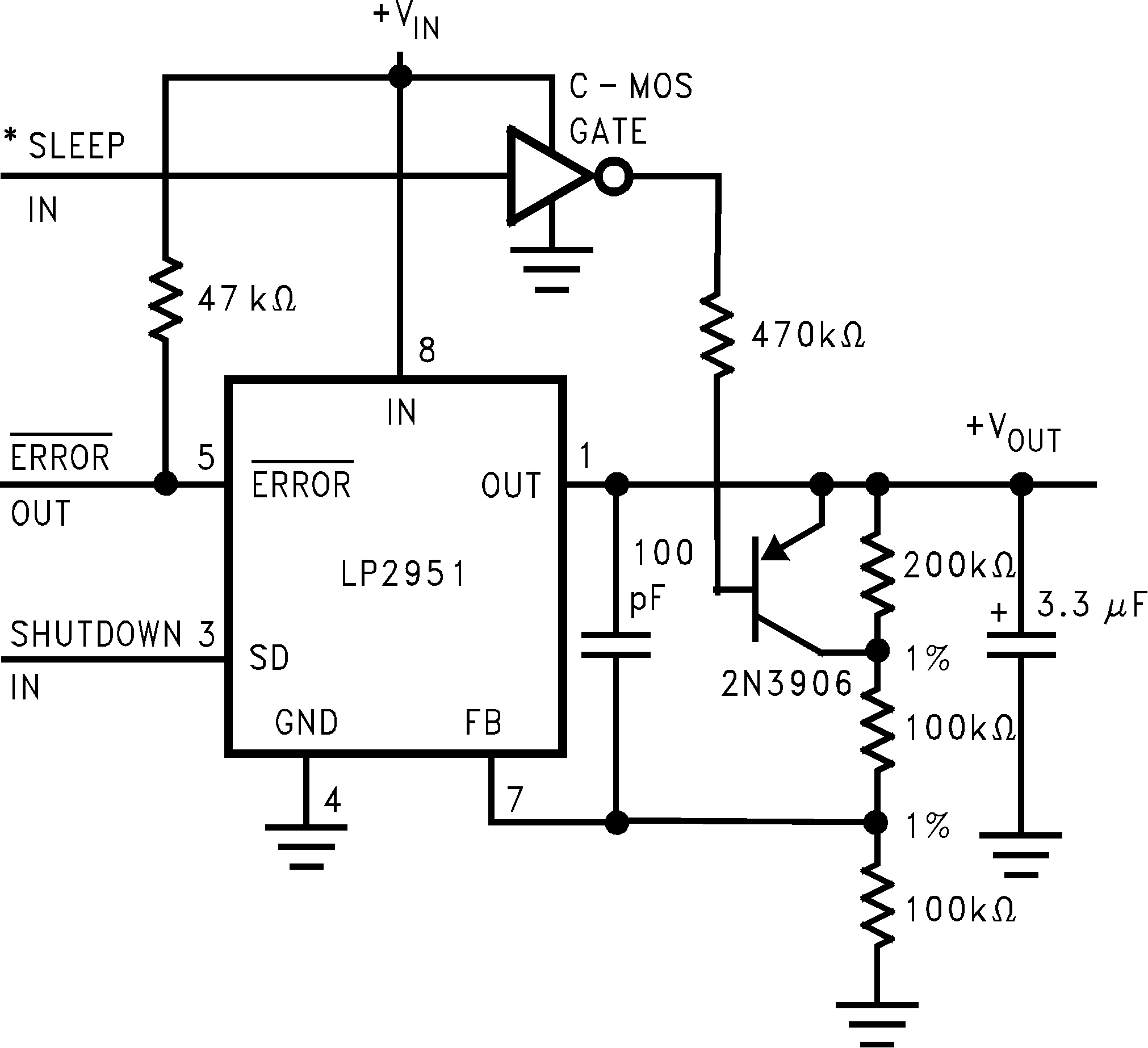
9.2.9 5-V Regulator with 2.5-V Sleep Function
In Figure 51, the 5-V regulator with 2.5-V sleep function works in below mode:
When sleep input is low, C-MOS output a high voltage and 2N3906 is off, then Vout = (1 + 300 KΩ/100 KΩ) × VFB ≈ 5 V
when sleep input is high, C-MOS output a low voltage, turns on 2N3906, then 200-KΩ resistor is bypassed from circuit, and VOUT = (1+100 KΩ/100 KΩ) × VFB ≈ 2.5 V.
9.2.10 Open Circuit Detector for 4 → 20-mA Current Loop
Figure 52 shows the open circuit detector for 4 → 20-mA current loop. The circuit outputs a high level while input current is less than 3.5 mA.
 Figure 52. Open Circuit Detector for 4 → 20-mA Current Loop
9.2.11 Regulator with State-of-Charge Indicator
In Figure 53, the LP339, a quad comparator, is used to indicate battery voltage state. The comparator’s negative input voltage is equal to the LP2951 1.235-V feedback voltage. By adjusting R3, we can adjust positive input voltage of C1~C3 to target value.

**Outputs go low when VIN drops below designated thresholds.
9.2.12 Low Battery Disconnect
In Figure 54, a band-gap voltage reference LM385 is used to generate shutdown signal, when Vin < 5.5 V, the LP2951 turns off and turns on again when VIN > 6 V.
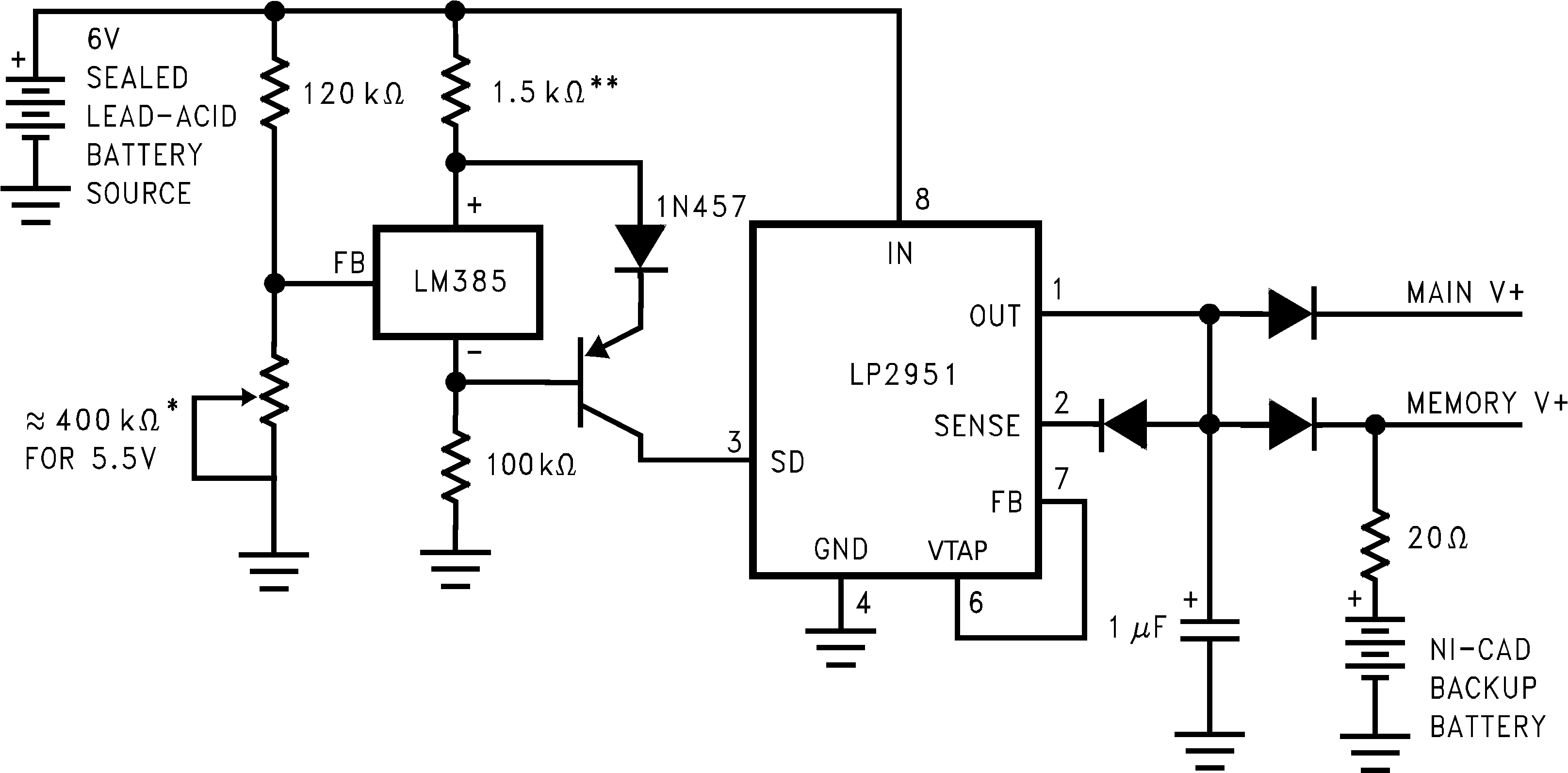
*Sets disconnect voltage.
**Sets disconnect hysteresis.
9.2.13 System Overtemperature Protection Circuit
In Figure 55, temperature sensors LM34/35's output voltage is linearly proportional to the Celsius (Centigrade) temperature.
At room temperature, LM34/35's output voltage is lower than 1.235-V feedback voltage, the internal pass transistor fully turns on, and the LP2951 output voltage is close to VIN.
When ambient temperature raise higher than protection target, LM34/35's output voltage is higher than 1.235-V feedback voltage, the internal pass transistor turns off, and the LP2951 output goes off.

LM35 for 125°C shutdown