SNVS001F april   2000  – july 2023 LP2980-ADJ

PRODUCTION DATA  

  1.   1
  2. Features
  3. Applications
  4. Description
  5. Revision History
  6. Pin Configuration and Functions
  7. Specifications
    1. 6.1 Absolute Maximum Ratings
    2. 6.2 ESD Ratings
    3. 6.3 Recommended Operating Conditions
    4. 6.4 Thermal Information
    5. 6.5 Electrical Characteristics
    6. 6.6 Typical Characteristics
  8. Detailed Description
    1. 7.1 Overview
    2. 7.2 Functional Block Diagram
    3. 7.3 Feature Description
      1. 7.3.1 Output Enable
      2. 7.3.2 Dropout Voltage
      3. 7.3.3 Current Limit
      4. 7.3.4 Undervoltage Lockout (UVLO)
      5. 7.3.5 Output Pulldown
      6. 7.3.6 Thermal Shutdown
    4. 7.4 Device Functional Modes
      1. 7.4.1 Device Functional Mode Comparison
      2. 7.4.2 Normal Operation
      3. 7.4.3 Dropout Operation
      4. 7.4.4 Disabled
  9. Application and Implementation
    1. 8.1 Application Information
      1. 8.1.1 External Feedback Resistors
      2. 8.1.2 Recommended Capacitor Types
        1. 8.1.2.1 Recommended Capacitors for the New Chip
        2. 8.1.2.2 Recommended Capacitors for the Legacy Chip
      3. 8.1.3 Input and Output Capacitor Requirements
      4. 8.1.4 Feed-Forward Capacitor (CFF)
      5. 8.1.5 Reverse Current
      6. 8.1.6 Power Dissipation (PD)
      7. 8.1.7 Estimating Junction Temperature
    2. 8.2 Typical Application
      1. 8.2.1 Design Requirements
      2. 8.2.2 Detailed Design Procedure
        1. 8.2.2.1 Setting VOUT For the LP2980-ADJ LDO
        2. 8.2.2.2 ON/OFF Input Operation
      3. 8.2.3 Application Curves
    3. 8.3 Power Supply Recommendations
    4. 8.4 Layout
      1. 8.4.1 Layout Guidelines
      2. 8.4.2 Layout Example
  10. Device and Documentation Support
    1. 9.1 Device Support
      1. 9.1.1 Device Nomenclature
    2. 9.2 Receiving Notification of Documentation Updates
    3. 9.3 Support Resources
    4. 9.4 Trademarks
    5. 9.5 Electrostatic Discharge Caution
    6. 9.6 Glossary
  11. 10Mechanical, Packaging, and Orderable Information

Package Options

Mechanical Data (Package|Pins)
Thermal pad, mechanical data (Package|Pins)
Orderable Information

Application Curves

at operating temperature TJ = 25°C, VIN = VOUT(NOM) + 1.0 V or 2.5 V (whichever is greater), IOUT = 1 mA, ON/OFF pin tied to VIN, CIN = 1.0 µF, and COUT = 4.7 µF (unless otherwise noted)
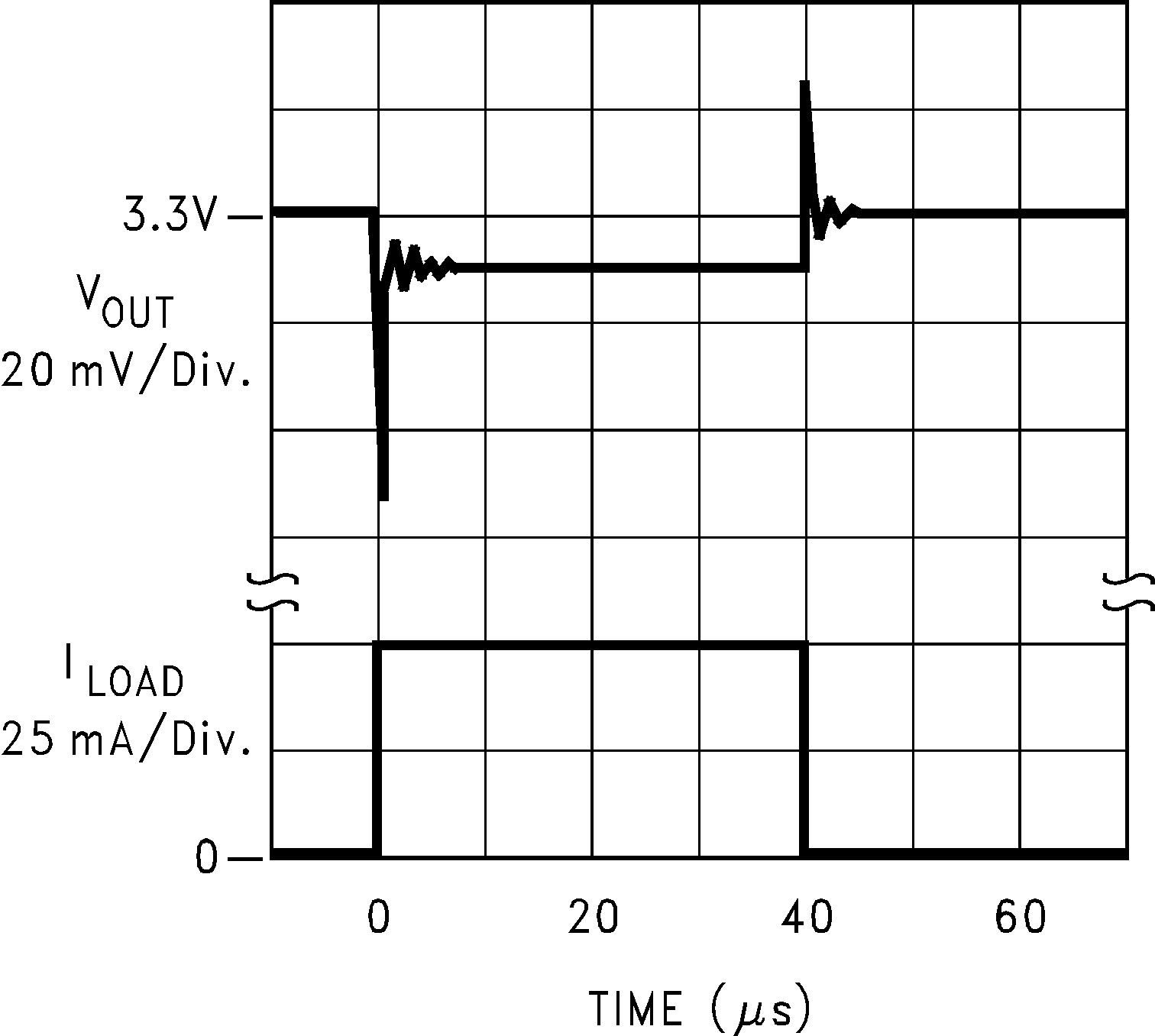
GUID-C5D1C0B6-F4EC-49F3-9101-9B2594ACD365-low.png
 
Figure 8-3 Load Transient Response for Legacy Chip
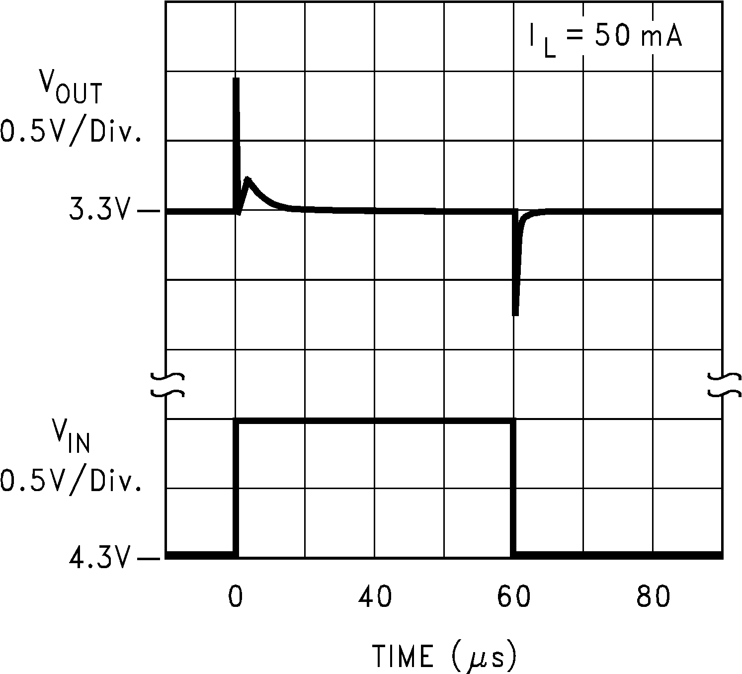
GUID-557C3FFD-54CC-4442-85C6-143D6BA320A4-low.png
 
Figure 8-5 Line Transient Response for Legacy Chip
GUID-20230619-SS0I-LRCV-BQDV-JWXXPN5ZTNZD-low.svg
VOUT = 3.3 V, dV/dt = 1 V/μs
Figure 8-7 Start-Up vs CFF for New Chip
GUID-20230619-SS0I-HZJW-BRNS-1G5RTVF7QTSM-low.svg
dI/dt = 1 A/μF
Figure 8-4 Load Transient Response for New Chip
GUID-20230619-SS0I-2PNJ-LPS4-ZRPNTCZZSLMB-low.svg
VOUT = 3.3 V, ΔVIN = 1 V, IOUT = 50 mA, dV/dt = 1 V/μs
Figure 8-6 Line Transient Response for New Chip