SNVS128L March   2000  – December 2023 LP2982

PRODUCTION DATA  

  1.   1
  2. Features
  3. Applications
  4. Description
  5. Pin Configuration and Functions
  6. Specifications
    1. 5.1 Absolute Maximum Ratings
    2. 5.2 ESD Ratings
    3. 5.3 Recommended Operating Conditions
    4. 5.4 Thermal Information
    5. 5.5 Electrical Characteristics
    6. 5.6 Typical Characteristics
  7. Detailed Description
    1. 6.1 Overview
    2. 6.2 Functional Block Diagram
    3. 6.3 Feature Description
      1. 6.3.1 Output Enable
      2. 6.3.2 Dropout Voltage
      3. 6.3.3 Current Limit
      4. 6.3.4 Undervoltage Lockout (UVLO)
      5. 6.3.5 Output Pulldown
      6. 6.3.6 Thermal Shutdown
    4. 6.4 Device Functional Modes
      1. 6.4.1 Device Functional Mode Comparison
      2. 6.4.2 Normal Operation
      3. 6.4.3 Dropout Operation
      4. 6.4.4 Disabled
  8. Application and Implementation
    1. 7.1 Application Information
      1. 7.1.1 Recommended Capacitor Types
        1. 7.1.1.1 Recommended Capacitors for the Legacy Chip
        2. 7.1.1.2 Recommended Capacitors for the New Chip
      2. 7.1.2 Input and Output Capacitor Requirements
      3. 7.1.3 Noise Bypass Capacitor (CBYPASS)
      4. 7.1.4 Reverse Current
      5. 7.1.5 Power Dissipation (PD)
      6. 7.1.6 Estimating Junction Temperature
    2. 7.2 Typical Application
      1. 7.2.1 Design Requirements
      2. 7.2.2 Detailed Design Procedure
        1. 7.2.2.1 ON/ OFF Input Operation
      3. 7.2.3 Application Curves
  9. Power Supply Recommendations
  10. Layout
    1. 9.1 Layout Guidelines
    2. 9.2 Layout Example
  11. 10Device and Documentation Support
    1. 10.1 Device Nomenclature
    2. 10.2 Third-Party Products Disclaimer
    3. 10.3 Documentation Support
      1. 10.3.1 Related Documentation
    4. 10.4 Receiving Notification of Documentation Updates
    5. 10.5 Support Resources
    6. 10.6 Trademarks
    7. 10.7 Electrostatic Discharge Caution
    8. 10.8 Glossary
  12. 11Revision History
  13. 12Mechanical, Packaging, and Orderable Information

Package Options

Mechanical Data (Package|Pins)
Thermal pad, mechanical data (Package|Pins)
Orderable Information

Application Curves

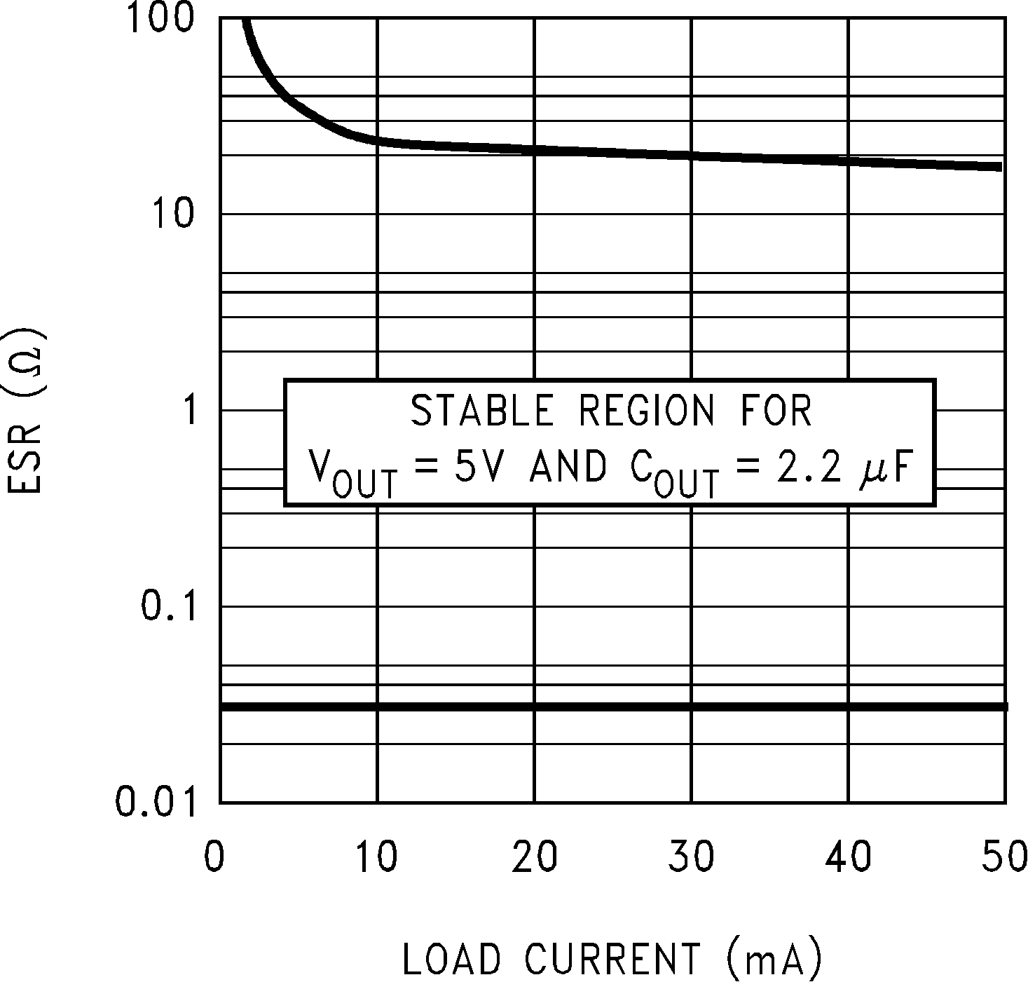
GUID-871DE464-FCCE-4230-8CFF-45155093A792-low.png
VIN = 6 V
Figure 7-3 5-V, 2.2-μF ESR Curves (Legacy chip)
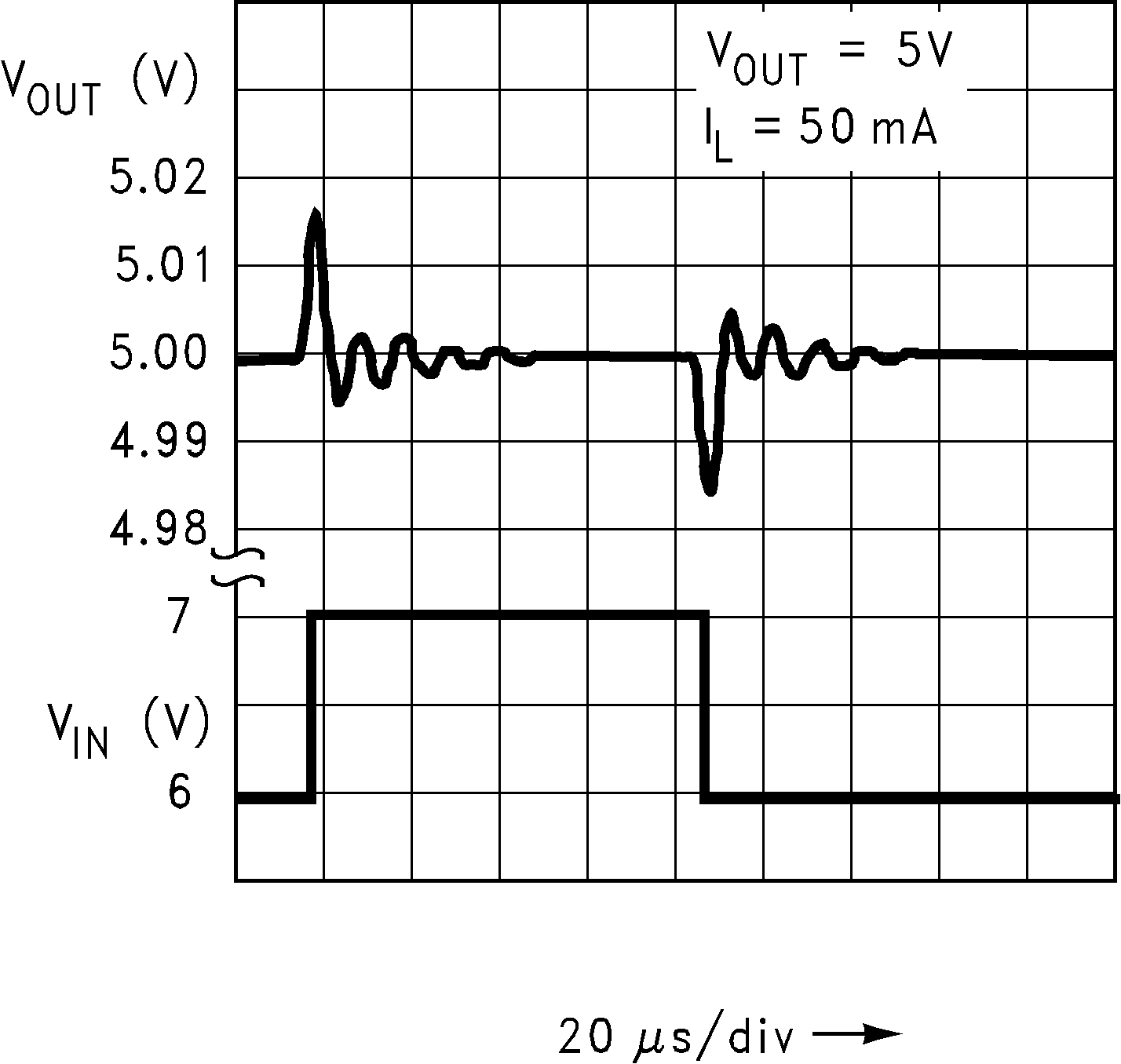
GUID-787F3DC7-6885-4FC4-A418-ADCB1631AF1B-low.png
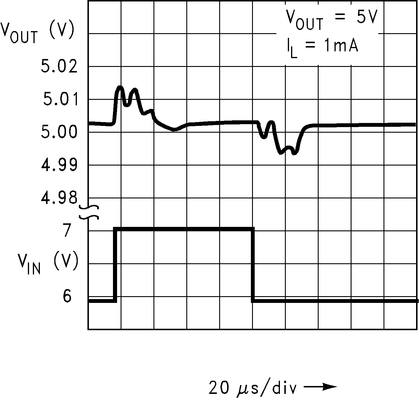
Figure 7-5 Line Transient Response (Legacy chip)
GUID-20230619-SS0I-2PNJ-LPS4-ZRPNTCZZSLMB-low.svg
VOUT = 3.3 V, ΔVIN = 1 V, IOUT = 50 mA, dV/dt = 1 V/μs
Figure 7-7 Line Transient Response (New Chip)
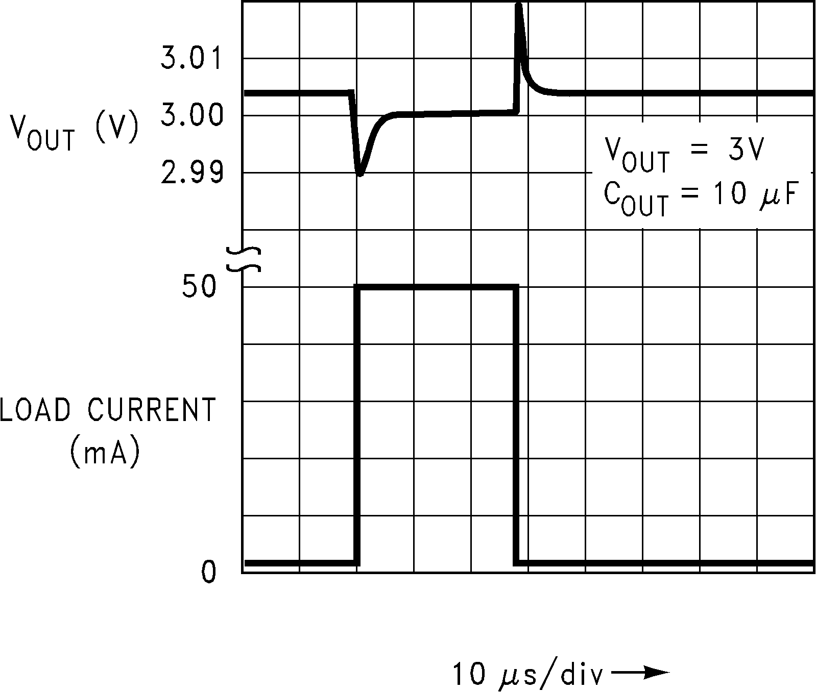
GUID-97D3D6FA-2161-42F7-8D45-027E7D24C11E-low.png
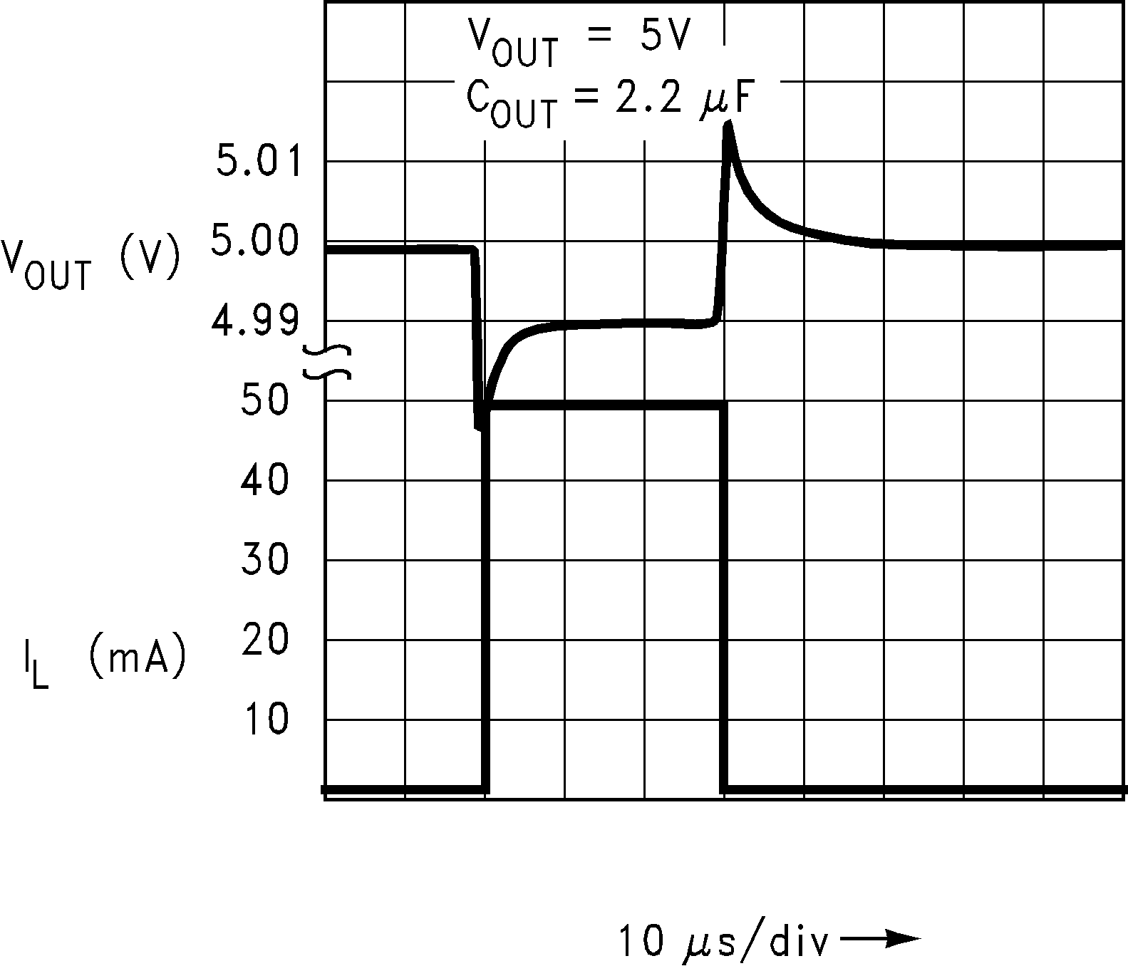
Figure 7-9 Load Transient Response (Legacy chip)
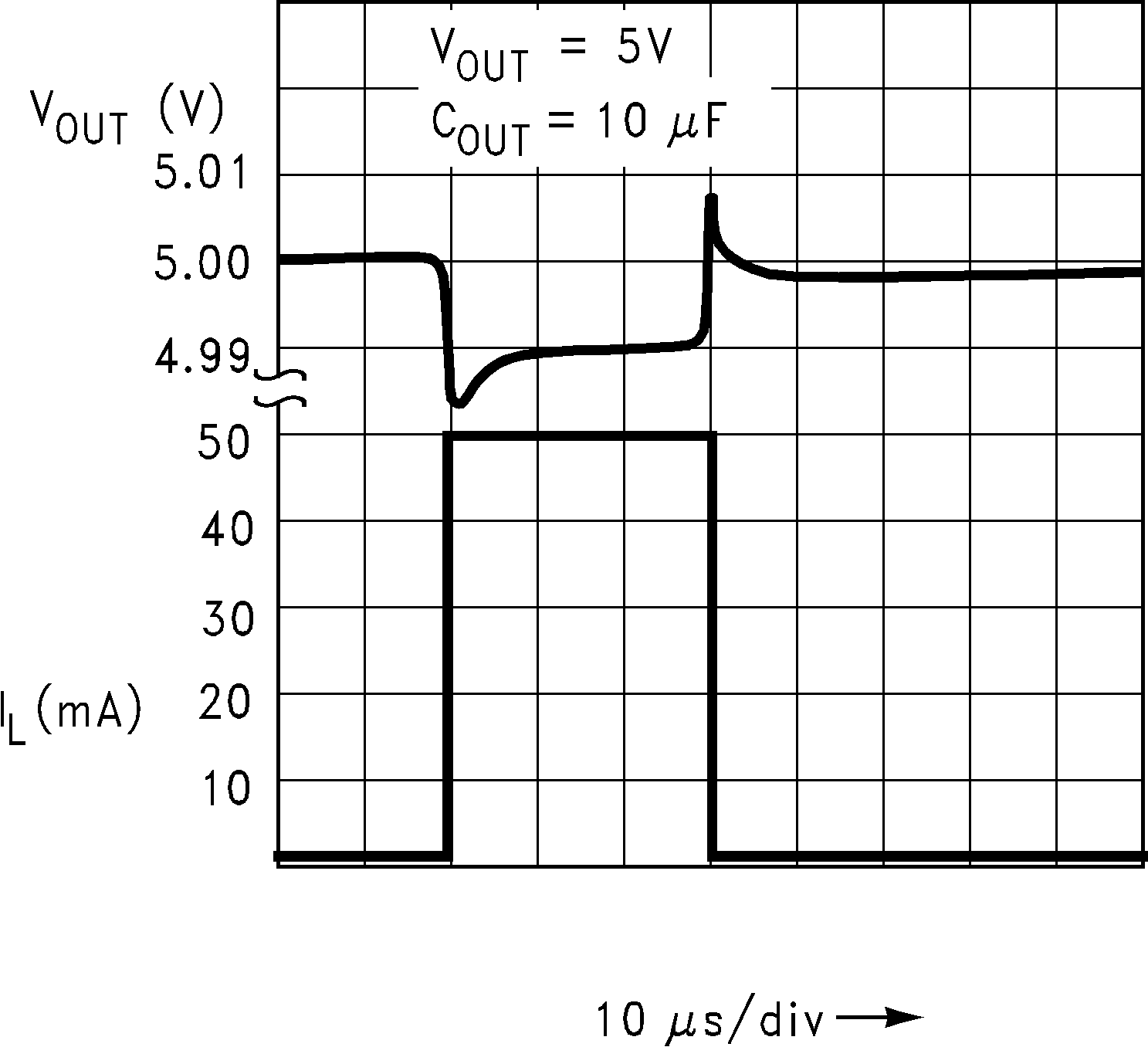
GUID-FAD6FD6A-A4B2-422F-A884-27E0BBA36AC3-low.png
Figure 7-11 Load Transient Response (Legacy chip)
GUID-75460937-EA6A-4D32-A7FE-217D4C3EBAA9-low.png
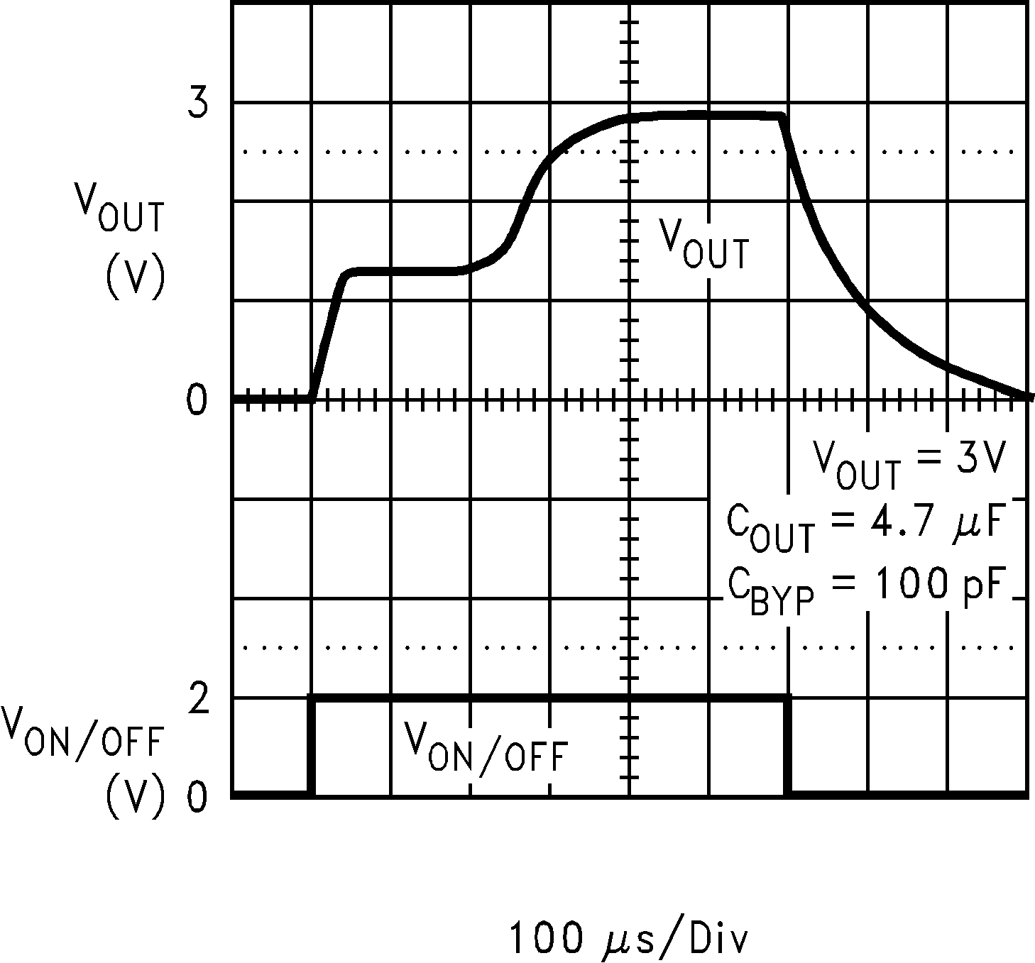
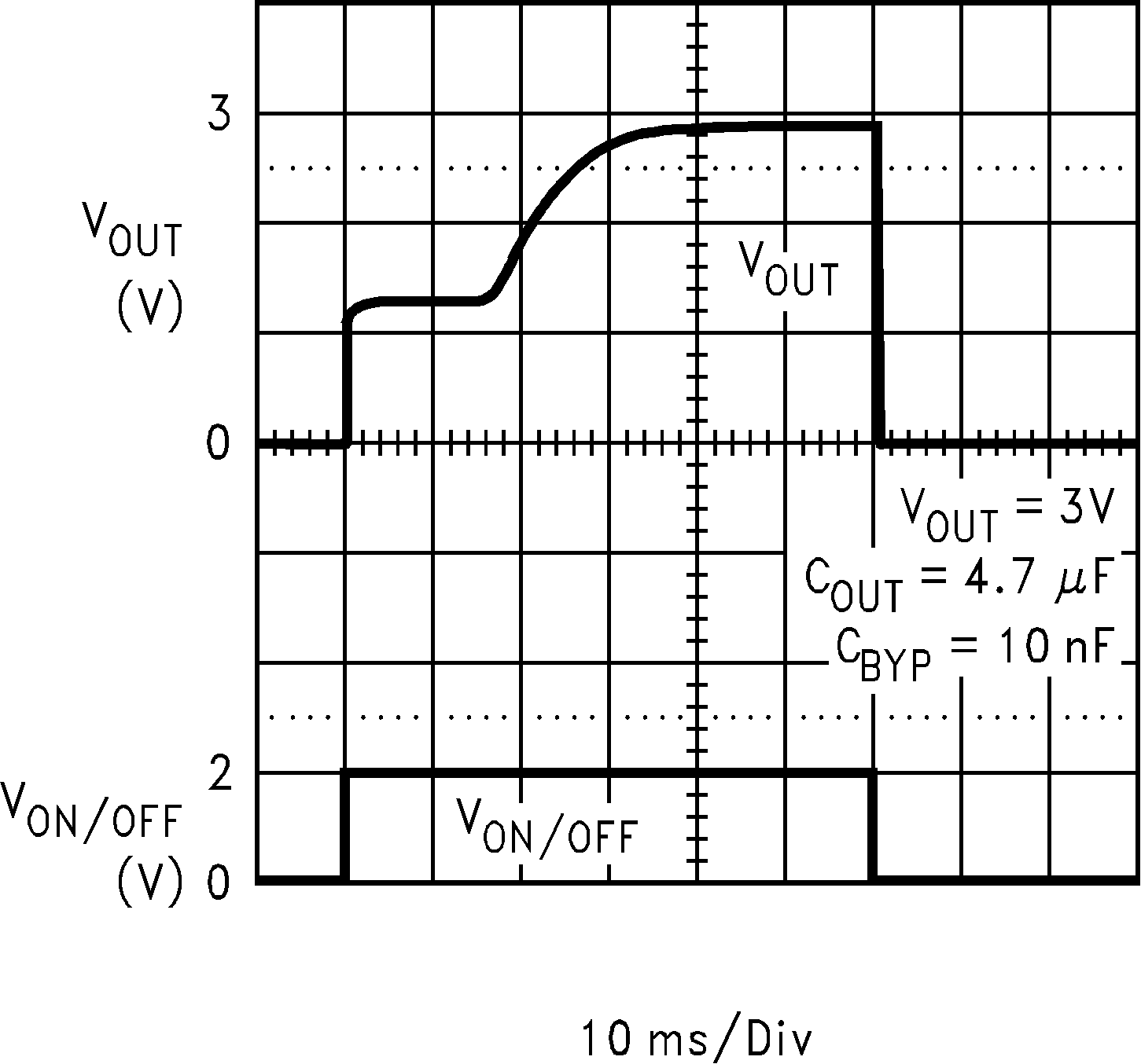
Figure 7-13 Turnon Waveform (Legacy chip)
GUID-704188A3-0998-4404-993D-BD81B6E61583-low.png
Figure 7-15 Turnon Waveform (Legacy chip)
GUID-20231128-SS0I-PTF7-MFF8-B8HKWDHF84N5-low.svg
Cbyp = 0.1 nF
Figure 7-17 Turnon Waveform (New chip)
GUID-67651E7E-78E0-4DDD-AF00-73FE0530EB60-low.png
VIN = 4 V
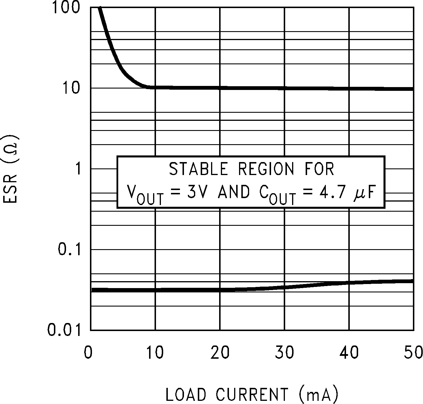
Figure 7-4 3-V, 4.7-μF ESR Curves (Legacy chip)
GUID-A691250E-435E-402A-896C-206CF41AE5C0-low.png
Figure 7-6 Line Transient Response (Legacy chip)
GUID-E43B7663-443C-4E7C-A040-B5B1DE58D459-low.png
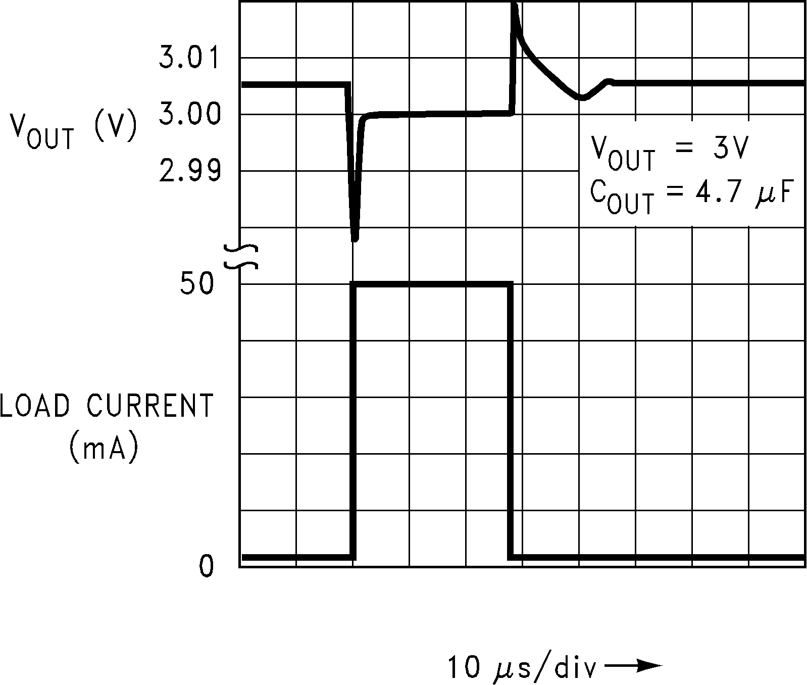
Figure 7-8 Load Transient Response (Legacy chip)
GUID-85C61F29-2310-4EB1-8CB5-4D71DF845A29-low.png
Figure 7-10 Load Transient Response (Legacy chip)
GUID-20230619-SS0I-HZJW-BRNS-1G5RTVF7QTSM-low.svg
dI/dt = 1 A/μs
Figure 7-12 Load Transient Response (New Chip)
GUID-6CD0E335-7AD5-4763-AED1-6D00E27B45B4-low.png
Figure 7-14 Turnon Waveform (Legacy chip)
GUID-20231128-SS0I-JD3B-KQ3D-XPTW1CTJCQRX-low.svg
Cbyp = 0 nF
Figure 7-16 Turnon Waveform (New chip)
GUID-20231128-SS0I-F0ML-J371-RHRRPRNRMVFP-low.svg
Cbyp = 1 nF
Figure 7-18 Turnon Waveform (New chip)