SNVS137I March 1999 – September 2015 LP2986
PRODUCTION DATA.
- 1 Features
- 2 Applications
- 3 Description
- 4 Revision History
- 5 Pin Configuration and Function
- 6 Specifications
- 7 Detailed Description
- 8 Application and Implementation
- 9 Power Supply Recommendations
- 10Layout
- 11Device and Documentation Support
- 12Mechanical, Packaging, and Orderable Information
Package Options
Mechanical Data (Package|Pins)
Thermal pad, mechanical data (Package|Pins)
Orderable Information
5 Pin Configuration and Function
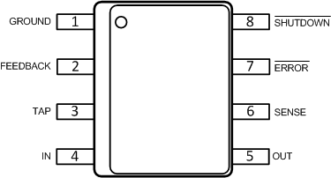
D Package
8-Pin SOIC
Top View

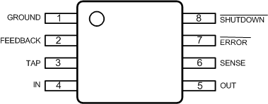
DGK Package
8-Pin VSSOP
Top View

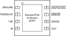
Pin Functions: All Packages
| PIN | I/O | DESCRIPTION | |
|---|---|---|---|
| NAME | NO. | ||
| ERROR | 7 | O | Active-low open-collector error output. Goes low when VOUT drops by 5% of its nominal value. |
| FEEDBACK | 2 | I | Determines the output voltage. Connect to TAP (with OUT tied to SENSE) to output the fixed voltage corresponding to the part version, or connect to a resistor divider to adjust the output voltage (see Typical Applications). |
| GROUND | 1 | — | Ground. |
| IN | 4 | I | Input voltage supply. |
| OUT | 5 | O | Regulated output. |
| SENSE | 6 | I | Connect to OUT (with FEEDBACK tied to TAP) to output the voltage corresponding to the part version (see Typical Applications). |
| SHUTDOWN | 8 | I | Active-high. pull low to showdown the output voltage. |
| TAP | 3 | O | Middle tap of the Internal voltage divider. Tie to FEEDBACK (with OUT tied to SENSE) to output the fixed voltage corresponding to the part version (see Typical Applications). |
| DAP (Thermal Pad - WSON only) | √ | — | The exposed thermal pad on the bottom of the WSON package should be connected to a copper thermal pad on the PCB under the package. The use of thermal vias to remove heat from the package into the PCB is recommended. Connect the thermal pad to ground potential or leave floating. Do not connect the thermal pad to any potential other than the same ground potential seen at device pin 1. For additional information on using TI's non-pullback WSON package, see Application Note AN-1187 Leadless Leadframe Package (LLP) (SNOA401). |
