SNVS083O February 2005 – March 2015 LP2989
PRODUCTION DATA.
- 1 Features
- 2 Applications
- 3 Description
- 4 Revision History
- 5 Pin Configuration and Functions
- 6 Specifications
- 7 Detailed Description
- 8 Application and Implementation
- 9 Power Supply Recommendations
- 10Layout
- 11Device and Documentation Support
- 12Mechanical, Packaging, and Orderable Information
Package Options
Mechanical Data (Package|Pins)
Thermal pad, mechanical data (Package|Pins)
Orderable Information
6 Specifications
6.1 Absolute Maximum Ratings
If Military/Aerospace specified devices are required contact the Texas Instruments Sales Office/Distributors for availability and specifications.(1)| MIN | MAX | UNIT | ||
|---|---|---|---|---|
| Operating junction temperature | –40 | 125 | °C | |
| Power dissipation(2) | Internally Limited | |||
| Input supply voltage | Survival | –0.3 | 16 | V |
| SENSE pin | –0.3 | 6 | V | |
| Output voltage | Survival(3) | –0.3 | 16 | V |
| IOUT (Survival) | Short-circuit protected | |||
| Input-output voltage | Survival(4) | –0.3 | 16 | V |
| Storage temperature range, Tstg | –65 | 150 | °C | |
(1) Stresses beyond those listed under Absolute Maximum Ratings may cause permanent damage to the device. These are stress ratings only, which do not imply functional operation of the device at these or any other conditions beyond those indicated under Recommended Operating Conditions. Exposure to absolute-maximum-rated conditions for extended periods may affect device reliability.
(2) The maximum allowable power dissipation is a function of the maximum junction temperature, TJ(MAX), the junction-to-ambient thermal resistance, RθJA, and the ambient temperature, TA. The maximum allowable power dissipation at any ambient temperature is calculated using: P(MAX) = (TJ(MAX) – TA) / RθJA. The value RθJA for the WSON (NGN) package is specifically dependent on PCB trace area, trace material, and the number of layers and thermal vias. For improved thermal resistance and power dissipation for the WSON package, refer to Application Note AN-1187 Leadless Leadframe Package (LLP) (SNOA401).. Exceeding the maximum allowable power dissipation will cause excessive die temperature, and the regulator will go into thermal shutdown.
(3) If used in a dual-supply system where the regulator load is returned to a negative supply, the LP2989 output must be diode-clamped to ground.
(4) The output PNP structure contains a diode between the IN and OUT pins that is normally reverse-biased. Forcing the output above the input will turn on this diode and may induce a latch-up mode which can damage the part.
6.2 ESD Ratings
| VALUE | UNIT | |||
|---|---|---|---|---|
| V(ESD) | Electrostatic discharge | Human-body model (HBM), per ANSI/ESDA/JEDEC JS-001(1) | ±2000 | V |
(1) JEDEC document JEP155 states that 500-V HBM allows safe manufacturing with a standard ESD control process.
6.3 Recommended Operating Conditions
over operating free-air temperature range (unless otherwise noted)| MIN | MAX | UNIT | ||
|---|---|---|---|---|
| Operating junction temperature | –40 | 125 | °C | |
| Operating input supply voltage | 2.1 | 16 | V | |
6.4 Thermal Information
| THERMAL METRIC(1) | LP2989 | UNIT | |||
|---|---|---|---|---|---|
| WSON (NGN) | SOIC (D) | VSSOP (DGK) | |||
| 8 PINS | 8 PINS | 8 PINS | |||
| RθJA | Junction-to-ambient thermal resistance, High-K | 34.8 | 114.5 | 156.5 | °C/W |
| RθJC(top) | Junction-to-case (top) thermal resistance | 28.4 | 61.1 | 51.0 | |
| RθJB | Junction-to-board thermal resistance | 12.0 | 55.6 | 76.5 | |
| ψJT | Junction-to-top characterization parameter | 0.2 | 9.7 | 4.9 | |
| ψJB | Junction-to-board characterization parameter | 12.2 | 54.9 | 75.2 | |
| RθJC(bot) | Junction-to-case (bottom) thermal resistance | 1.3 | n/a | n/a | |
(1) For more information about traditional and new thermal metrics, see the IC Package Thermal Metrics application report, SPRA953.
6.5 Electrical Characteristics
Unless otherwise specified: TJ = 25°C, VIN = VOUT(NOM) + 1 V, IOUT = 1 mA, COUT = 4.7 µF, CIN = 2.2 µF, VSD = 2 V.| PARAMETER | TEST CONDITIONS | LP2989AI-X.X(1) | LP2989I-X.X(1) | UNIT | |||||
|---|---|---|---|---|---|---|---|---|---|
| MIN | TYP | MAX | MIN | TYP | MAX | ||||
| VOUT | Output voltage tolerance | −0.75 | 0.75 | −1.25 | 1.25 | %VNOM | |||
| 1 mA < IOUT < 500 mA, VOUT(NOM) + 1 V ≤ VIN ≤ 16 V | −1.5 | 1.5 | −2.5 | 2.5 | |||||
| 1 mA < IOUT < 500 mA, VOUT(NOM) + 1 V ≤ VIN ≤ 16 V, –40°C ≤ TJ ≤ 125°C | −4 | 2.5 | −5 | 3.5 | |||||
| 1 mA < IOUT < 500 mA, VOUT(NOM) + 1 V ≤ VIN ≤ 16 V, −25°C ≤ TJ ≤ 125°C | −3.5 | 2.5 | −4.5 | 3.5 | |||||
| ΔVOUT/ΔVIN | Output voltage line regulation | VOUT(NOM) + 1 V ≤ VIN ≤ 16 V | 0.005 | 0.014 | 0.005 | 0.014 | %/V | ||
| VOUT(NOM) + 1 V ≤ VIN ≤ 16 V, –40°C ≤ TJ ≤ 125°C | 0.005 | 0.032 | 0.005 | 0.032 | |||||
| ΔVOUT/ΔIOUT | Load regulation | 1 mA < IOUT < 500 mA | 0.4 | 0.4 | %VNOM | ||||
| VIN – VOUT | Dropout voltage(2) | IOUT = 100 µA | 1 | 3 | 1 | 3 | mV | ||
| IOUT = 100 µA, –40°C ≤ TJ ≤ 125°C | 1 | 4 | 1 | 4 | |||||
| IOUT = 200 mA | 150 | 200 | 150 | 200 | mV | ||||
| IOUT = 200 mA, –40°C ≤ TJ ≤ 125°C | 150 | 300 | 150 | 300 | |||||
| IOUT = 500 mA | 310 | 425 | 310 | 425 | mV | ||||
| IOUT = 500 mA, –40°C ≤ TJ ≤ 125°C | 310 | 650 | 310 | 650 | |||||
| IGND | Ground pin current | IOUT = 100 µA | 110 | 175 | 110 | 175 | µA | ||
| IOUT = 100 µA, –40°C ≤ TJ ≤ 125°C | 110 | 200 | 110 | 200 | |||||
| IOUT= 200 mA | 1 | 2 | 1 | 2 | mA | ||||
| IOUT = 200 mA, –40°C ≤ TJ ≤ 125°C | 1 | 3.5 | 1 | 3.5 | |||||
| IOUT = 500 mA | 3 | 6 | 3 | 6 | mA | ||||
| IOUT = 500 mA, –40°C ≤ TJ ≤ 125°C | 3 | 9 | 3 | 9 | |||||
| VSD < 0.18 V, –40°C ≤ TJ ≤ 125°C | 0.5 | 2 | 0.5 | 2 | µA | ||||
| VSD < 0.4 V | 0.05 | 0.8 | 0.05 | 0.8 | |||||
| IOUT(PK) | Peak output current | VOUT ≥ VOUT(NOM) − 5% | 600 | 800 | 600 | 800 | mA | ||
| IOUT(MAX) | Short circuit current | RL = 0 (Steady State)(4) | 1000 | 1000 | mA | ||||
| en | Output noise voltage (RMS) | BW = 100 Hz to 100 kHz, COUT = 10 µF, CBYPASS = .01 µF, VOUT = 2.5 V | 18 | 18 | µV(RMS) | ||||
| ΔVOUT/ΔVIN | Ripple Rejection | f = 1 kHz, COUT = 10 µF | 60 | 60 | dB | ||||
| ΔVOUT/ΔTD | Output voltage temperature coefficient | See(3), –40°C ≤ TJ ≤ 125°C | 20 | 20 | ppm/°C | ||||
| SHUTDOWN INPUT | |||||||||
| VSD | SD Input voltage | VH = Output ON | 1.4 | 1.4 | V | ||||
| VH = Output ON, –40°C ≤ TJ ≤ 125°C | 1.6 | 1.6 | |||||||
| VL = Output OFF | 0.5 | 0.5 | |||||||
| VL = Output OFF, IIN ≤ 2 µA, –40°C ≤ TJ ≤ 125°C | 0.18 | 0.18 | |||||||
| ISD | SD Input current | VSD = 0 | 0.001 | 0.001 | µA | ||||
| VSD = 0, –40°C ≤ TJ ≤ 125°C | −1 | −1 | |||||||
| VSD = 5 V | 5 | 5 | |||||||
| VSD = 5 V, –40°C ≤ TJ ≤ 125°C | 15 | 15 | |||||||
| ERROR COMPARATOR | |||||||||
| IOH | Output “HIGH” leakage | VOH = 16 V | 0.001 | 1 | 0.001 | 1 | µA | ||
| VOH = 16 V, –40°C ≤ TJ ≤ 125°C | 0.001 | 2 | 0.001 | 2 | |||||
| VOL | Output “LOW” voltage | VIN = VOUT(NOM) − 0.5 V, IOUT(COMP) = 150 µA | 150 | 220 | 150 | 220 | mV | ||
| VIN = VOUT(NOM) − 0.5 V, IOUT(COMP) = 150 µA, –40°C ≤ TJ ≤ 125°C | 150 | 350 | 150 | 350 | |||||
| VTHR(MAX) | Upper threshold voltage | −6 | −4.8 | −3.5 | −6 | −4.8 | −3.5 | %VOUT | |
| –40°C ≤ TJ ≤ 125°C | −8.3 | −4.8 | −2.5 | −8.3 | −4.8 | −2.5 | |||
| VTHR(MIN) | Lower threshold voltage | −8.9 | −6.6 | −4.9 | −8.9 | −6.6 | −4.9 | %VOUT | |
| –40°C ≤ TJ ≤ 125°C | −13 | −6.6 | −3 | −13 | −6.6 | −3 | |||
| HYST | Hysteresis | 2 | |||||||
(1) Limits are 100% production tested at 25°C. Limits over the operating temperature range are specified through correlation using Statistical Quality Control (SQC) methods. The limits are used to calculate TI’s Average Outgoing Quality Level (AOQL).
(2) Dropout voltage is defined as the input to output differential at which the output voltage drops 100 mV below the value measured with a 1-V differential.
(3) Temperature coefficient is defined as the maximum (worst-case) change divided by the total temperature range.
(4) See the Typical Characteristics section.
6.6 Typical Characteristics
TA = 25°C, COUT = 4.7 µF, CIN = 2.2 µF, SD is tied to VIN, VIN = VOUT(NOM)+ 1 V, IOUT = 1 mA, VOUT = 2.5 V (unless otherwise specified)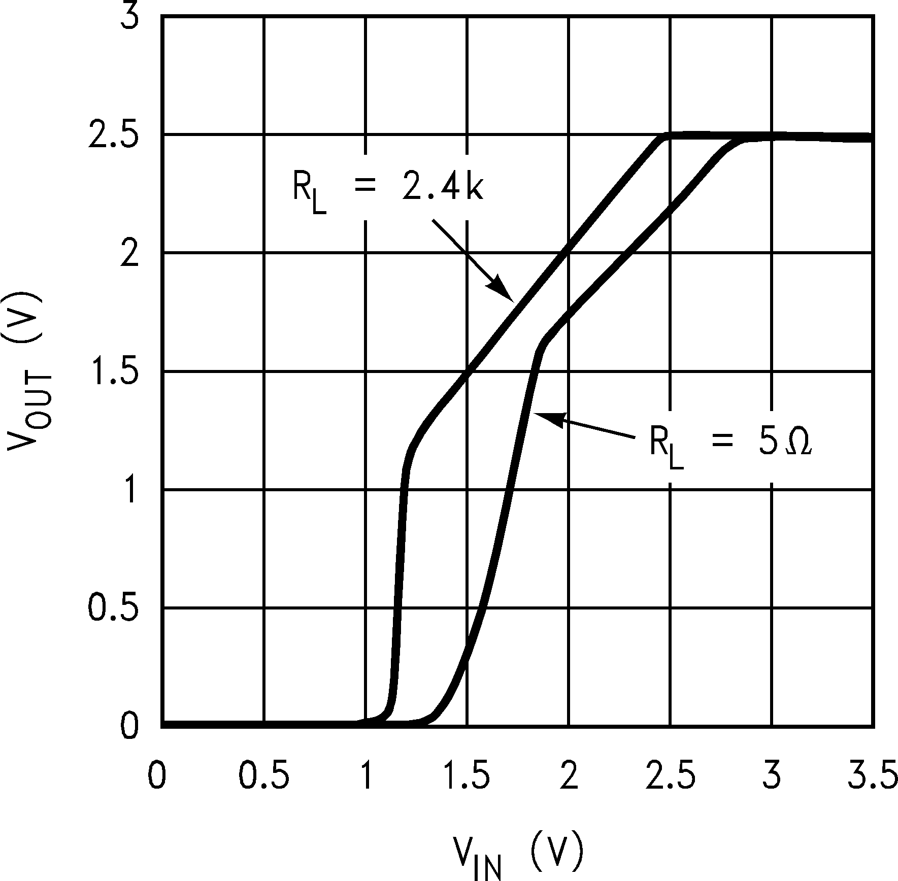 Figure 1. Dropout Characteristics
 Figure 3. Dropout Voltage vs Load Current
 Figure 5. Ground Pin Current vs Load Current
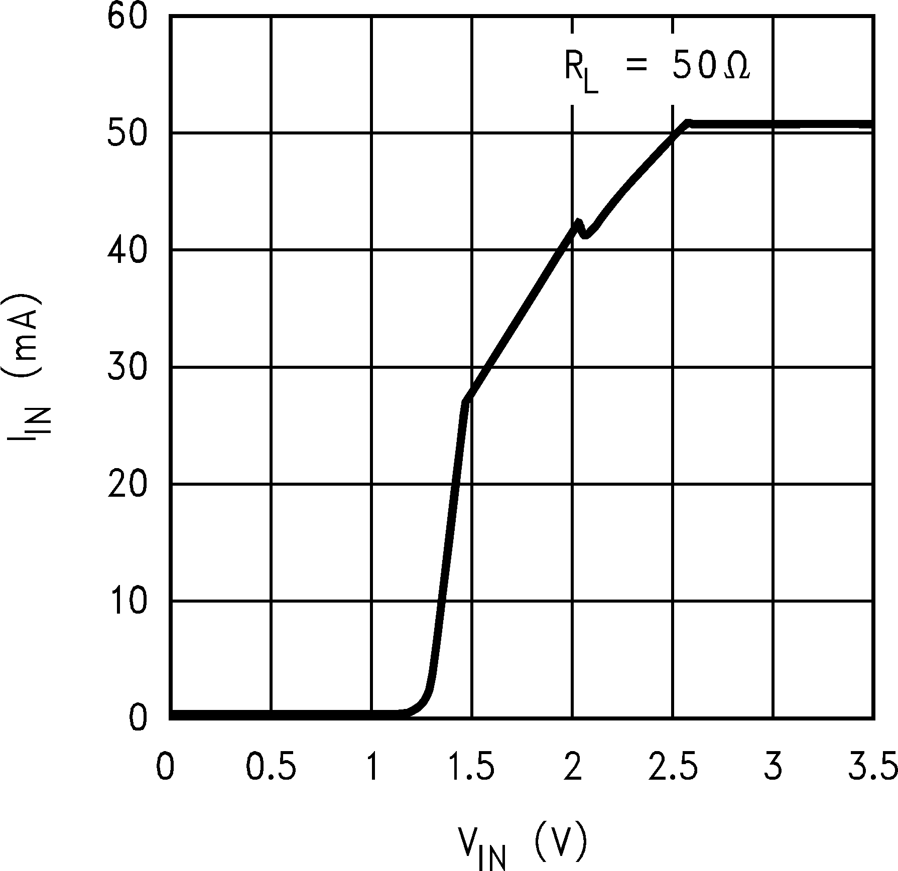 Figure 7. Input Current vs VIN
 Figure 9. Line Transient Response
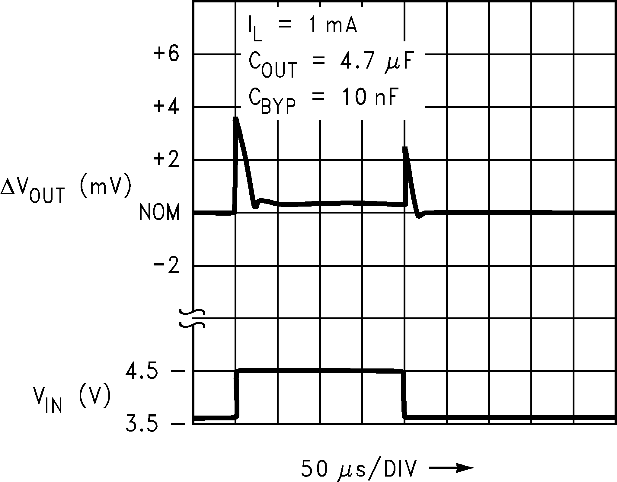 Figure 11. Line Transient Response
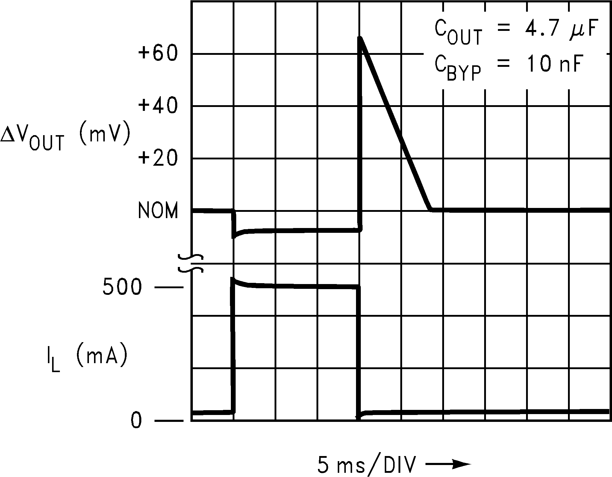 Figure 13. Load Transient Response
 Figure 15. Short Circuit Current
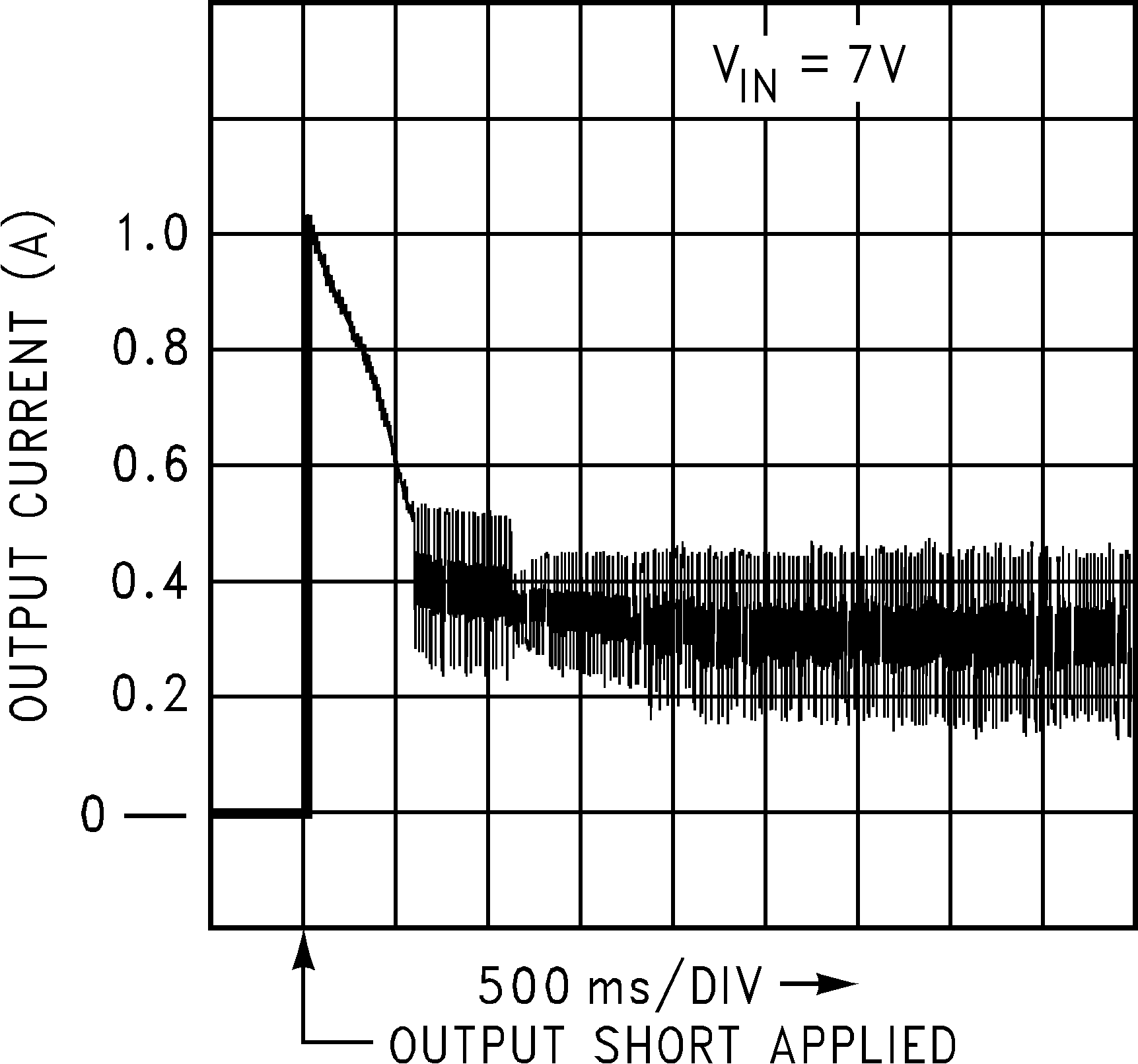 Figure 17. Short Circuit Current
 Figure 19. Ripple Rejection
 Figure 21. Ripple Rejection
 Figure 23. Ripple Rejection
 Figure 25. Ripple Rejection
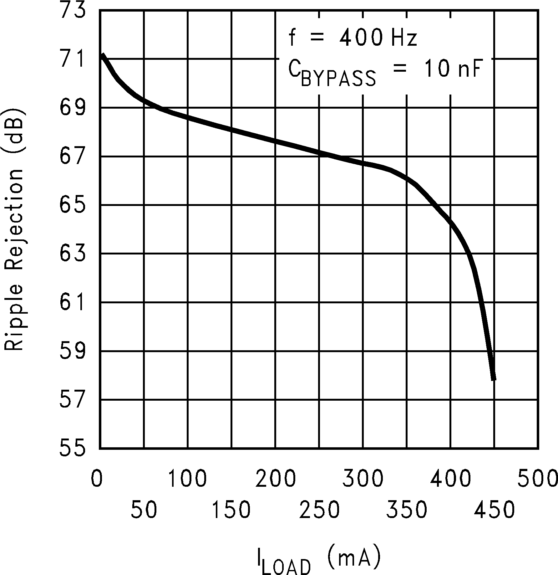 Figure 27. Ripple Rejection vs Load
 Figure 29. Output Noise Density
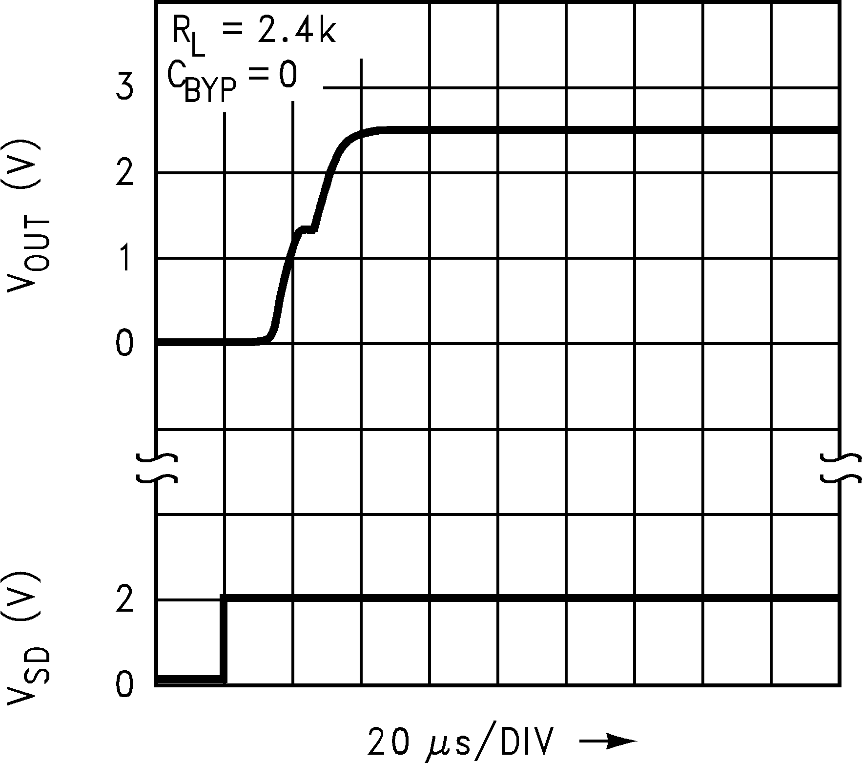 Figure 31. Turn-ON Waveform
 Figure 33. Turn-ON Waveform
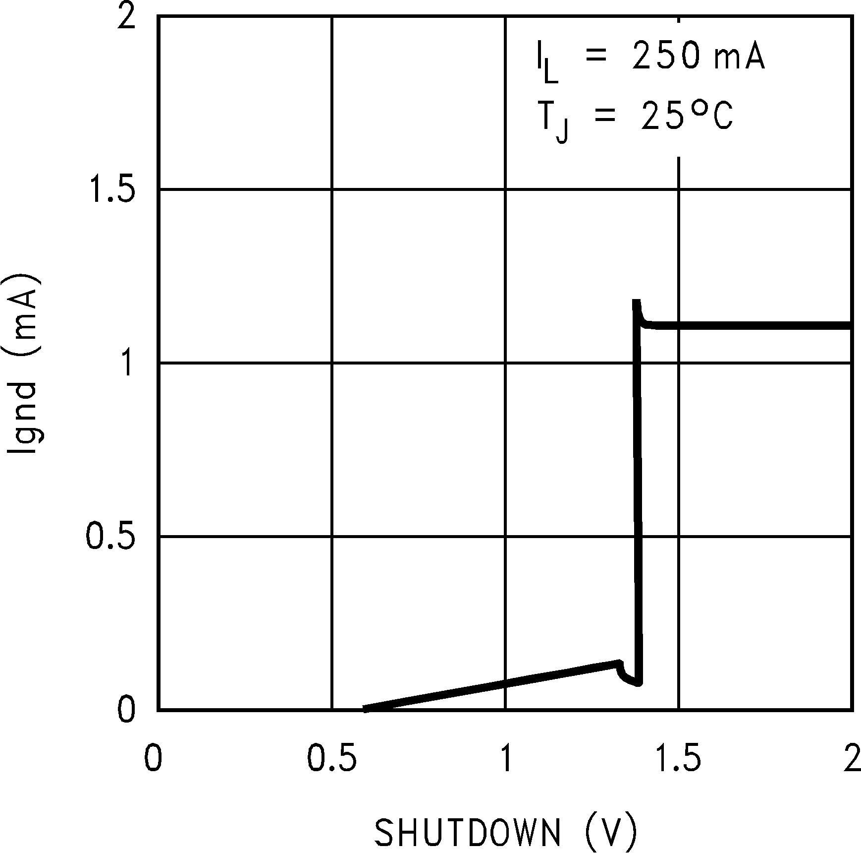 Figure 35. IGND vs Shutdown
 Figure 37. IGND vs Shutdown
 Figure 39. Typical Temperature vs VOUT (LP2989-2.5)
 Figure 2. Dropout Voltage vs Temperature
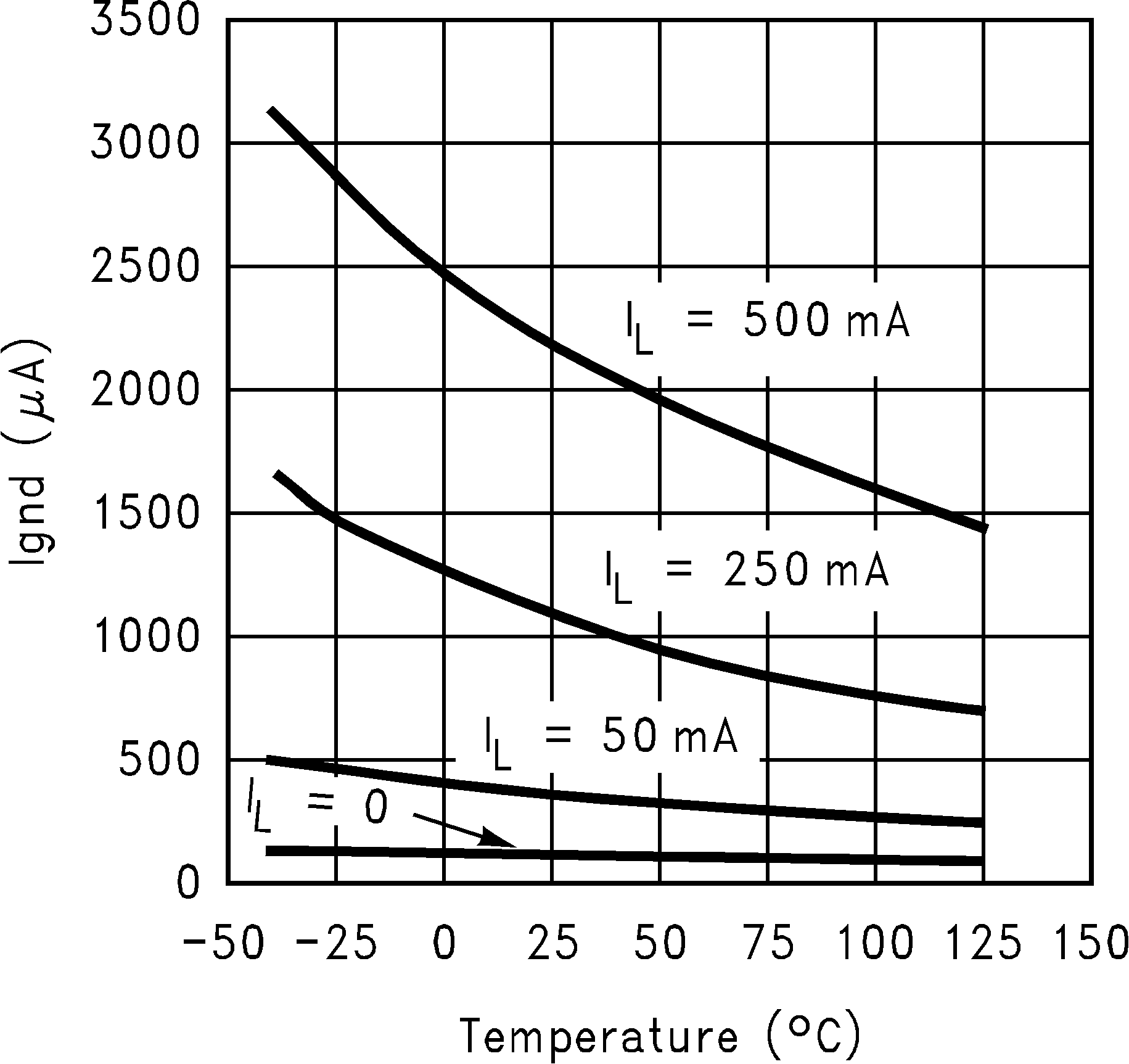 Figure 4. GND Pin Current vs Temperature and Load
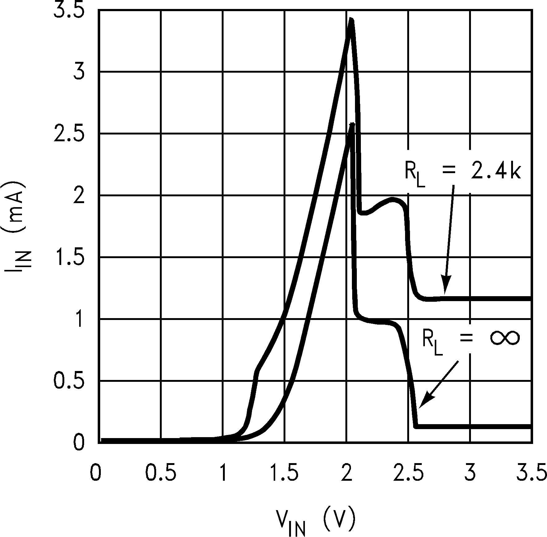 Figure 6. Input Current vs VIN
 Figure 8. Input Current vs VIN
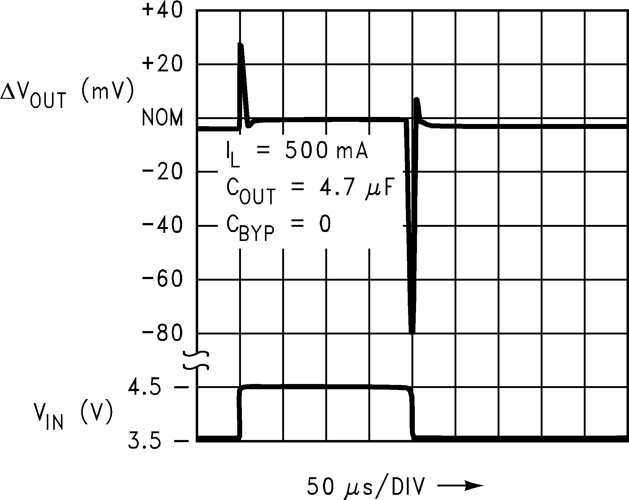 Figure 10. Line Transient Response
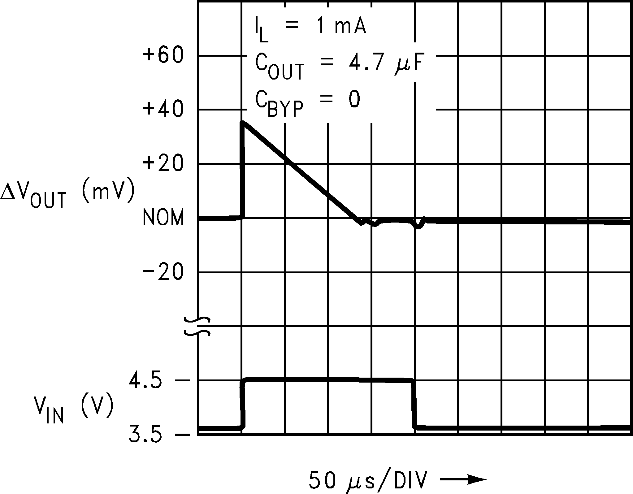 Figure 12. Line Transient Response
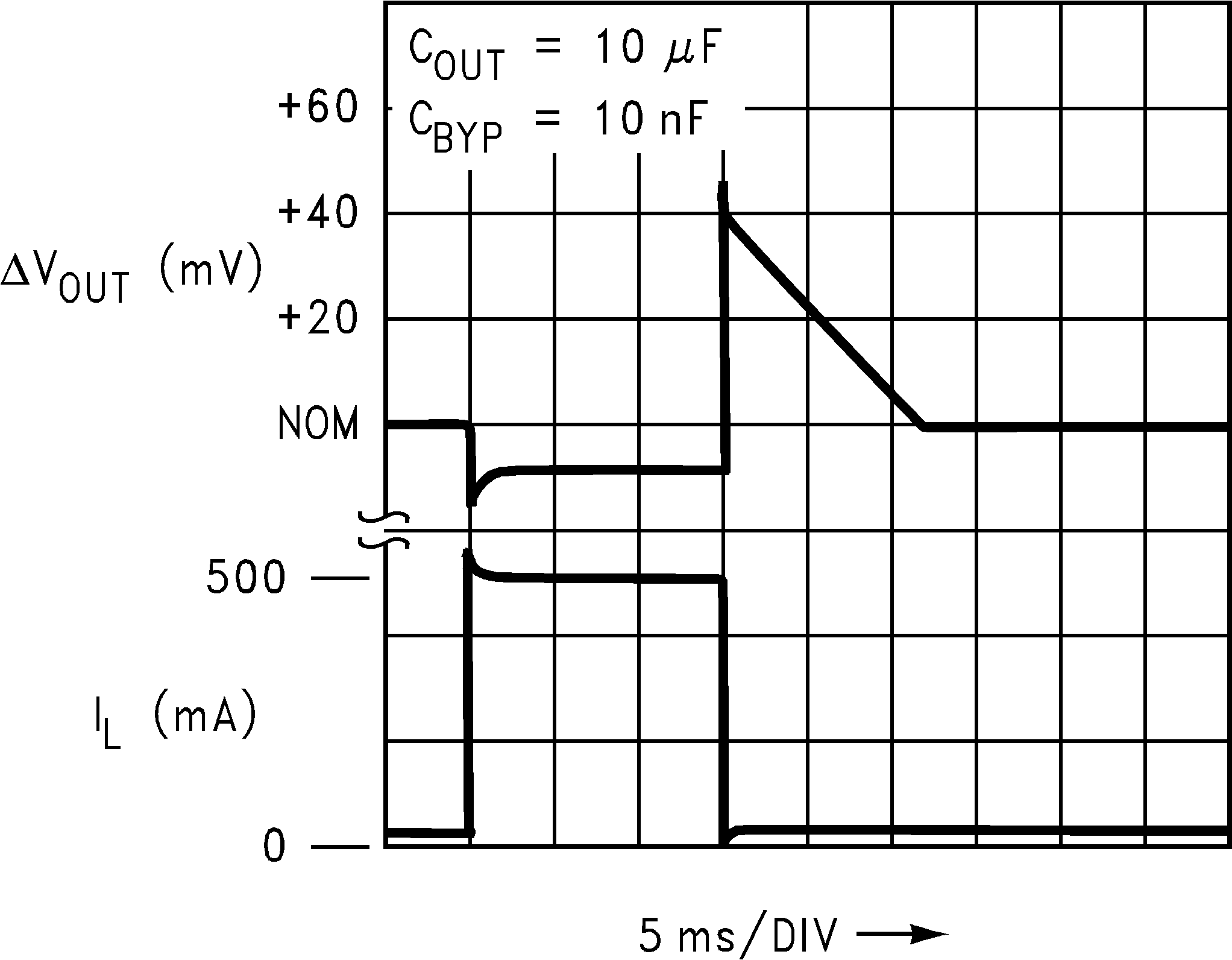 Figure 14. Load Transient Response
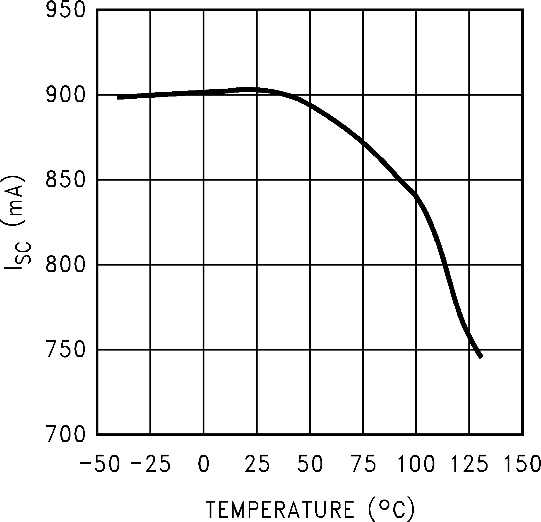 Figure 16. Short Circuit Current vs Temperature
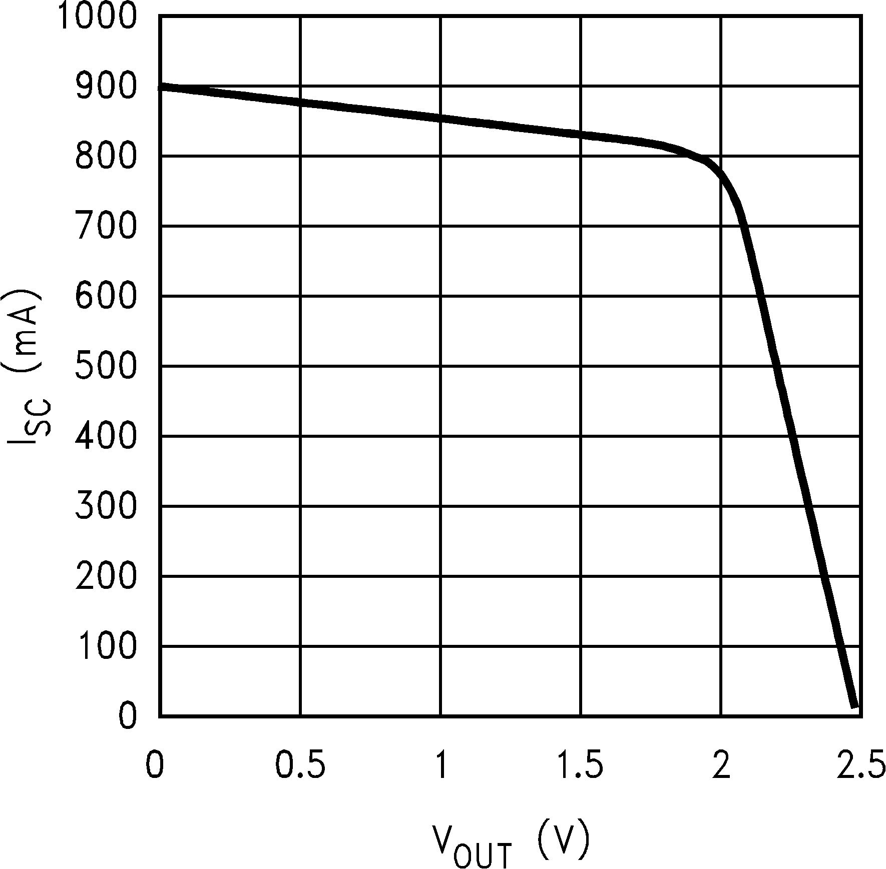 Figure 18. Short Circuit Current vs VOUT
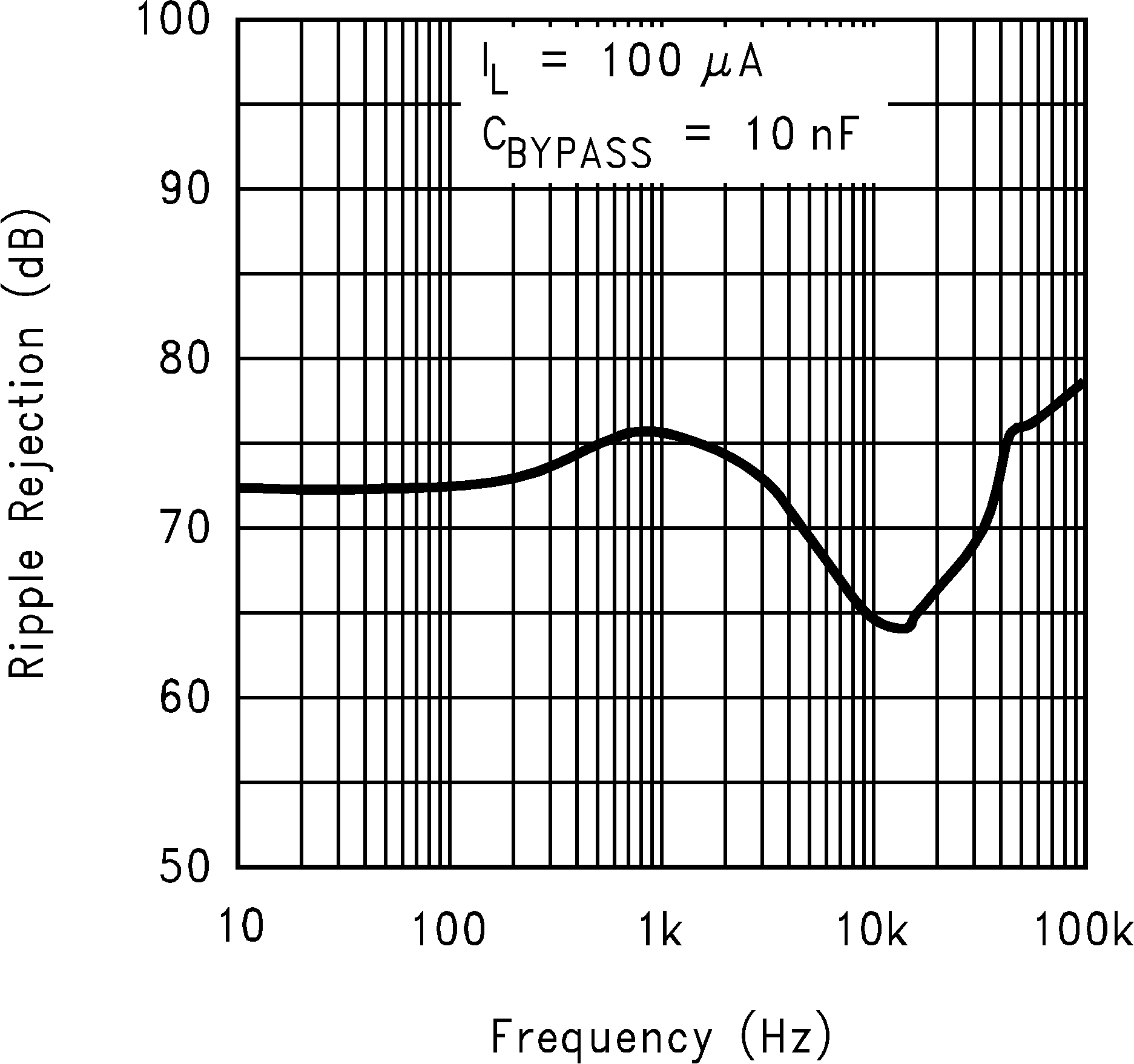 Figure 20. Ripple Rejection
 Figure 22. Ripple Rejection
 Figure 24. Ripple Rejection
 Figure 26. Ripple Rejection in Dropout
 Figure 28. Output Noise Density
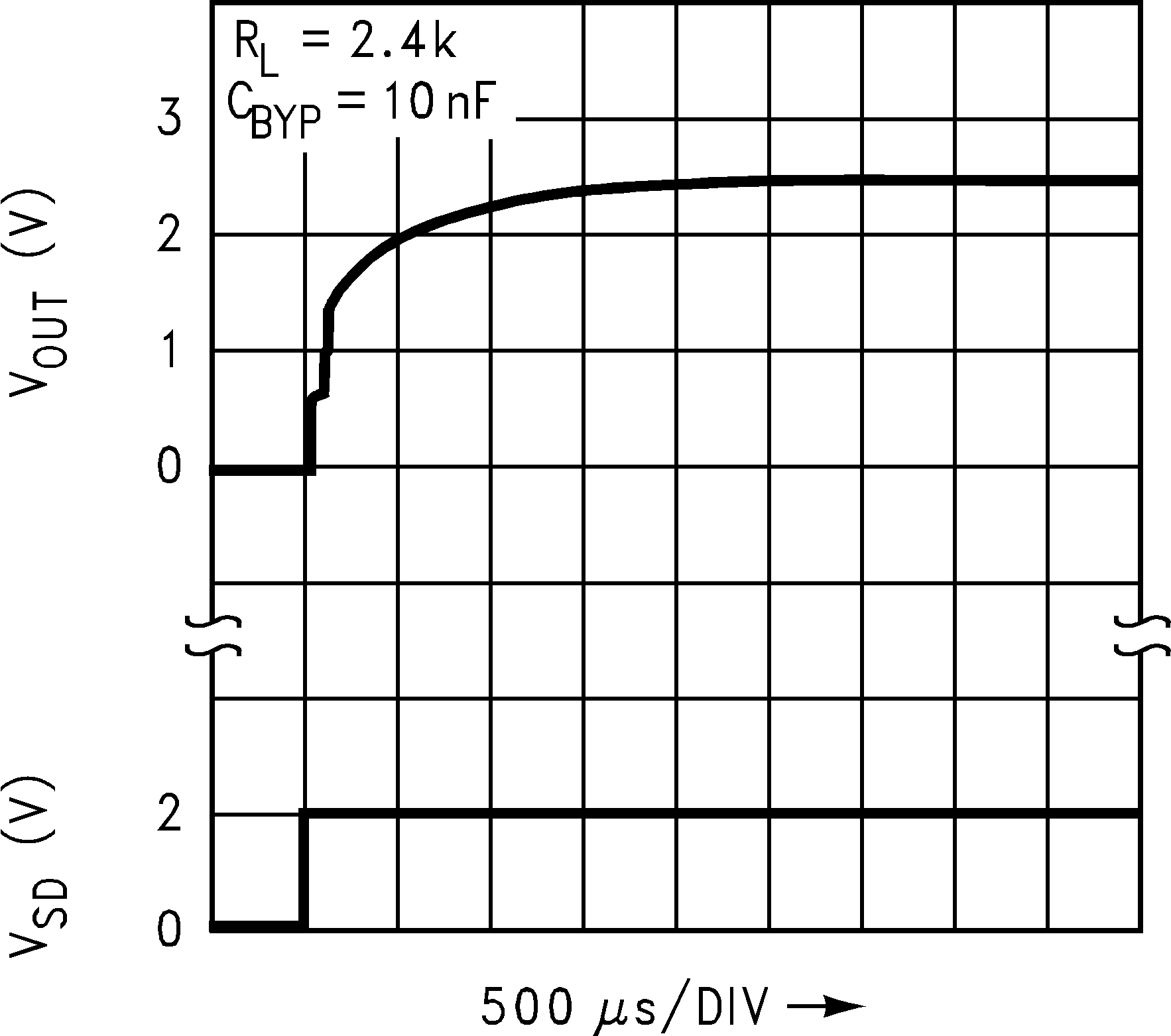 Figure 30. Turn-ON Waveform
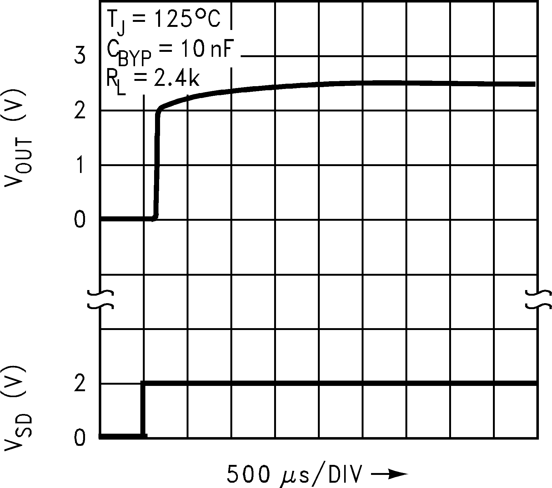 Figure 32. Turn-ON Waveform
 Figure 34. IGND vs Shutdown
 Figure 36. IGND vs Shutdown
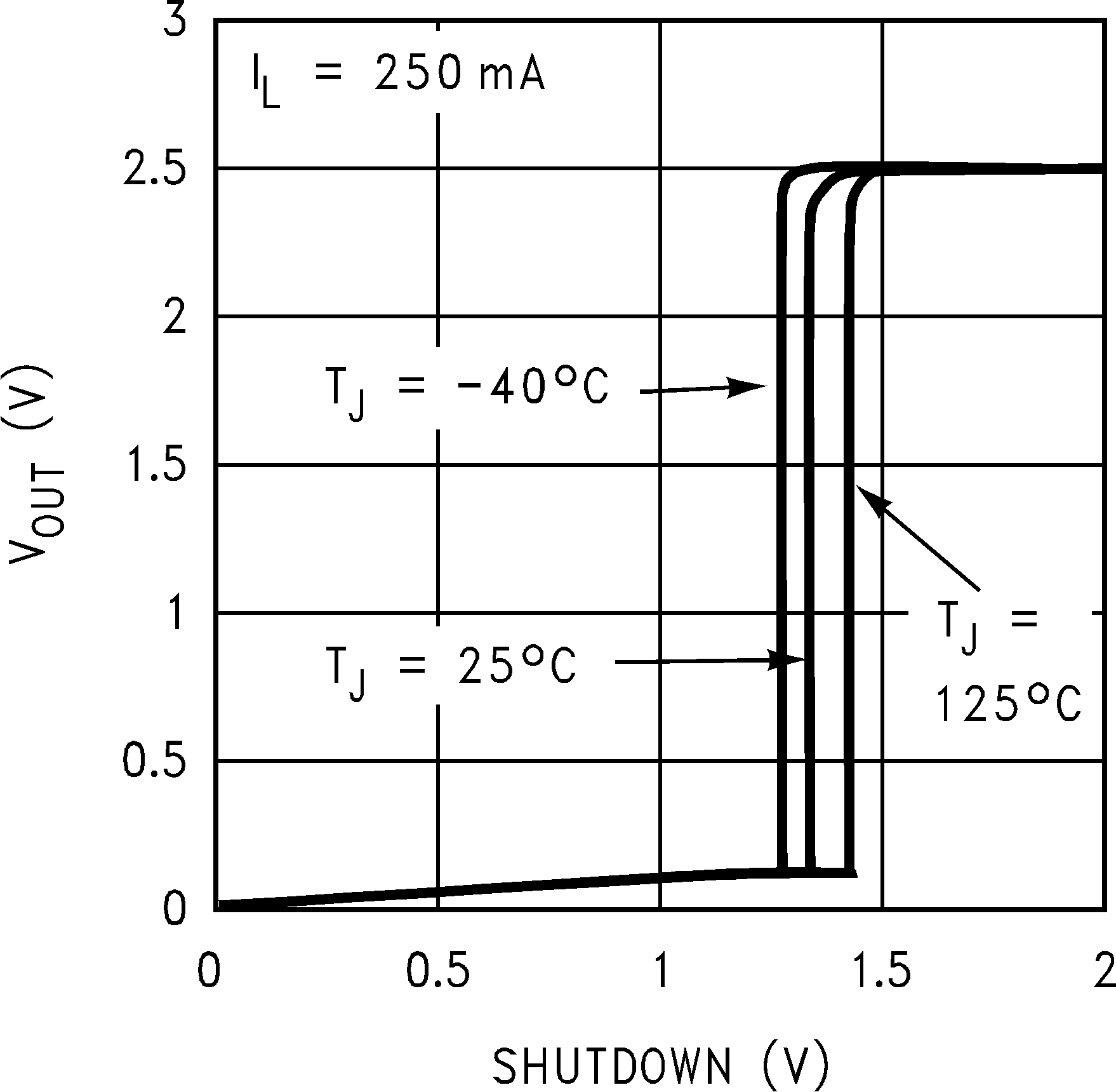 Figure 38. VOUT vs Shutdown