CIN = 1µF, COUT =
4.7µF, VIN = VOUT(NOM) + 1V, TA = 25°C, and
ON/OFF pin is tied to the IN pin (unless otherwise noted)
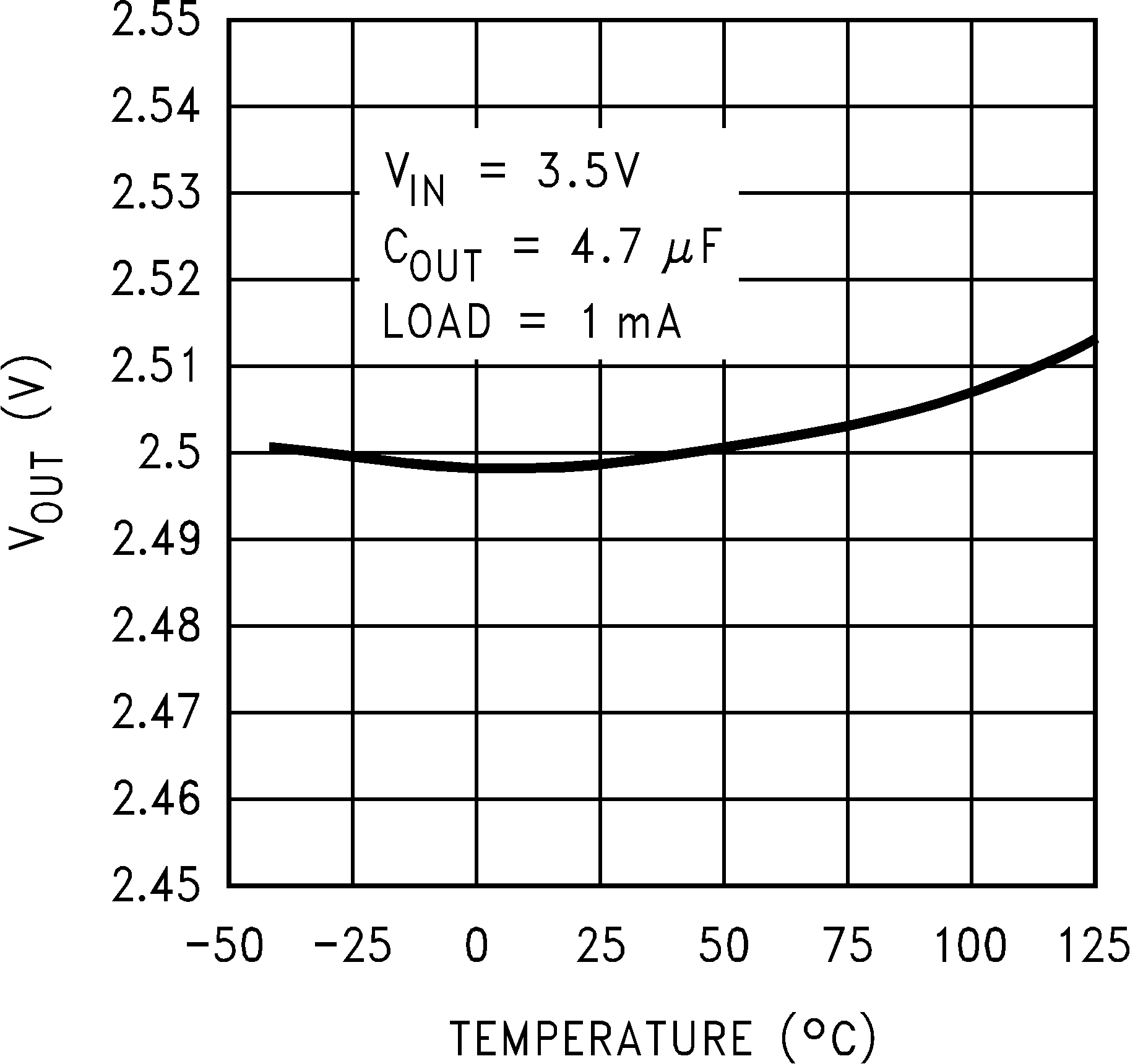 Figure 5-1 VOUT
vs Temperature (Legacy Chip)
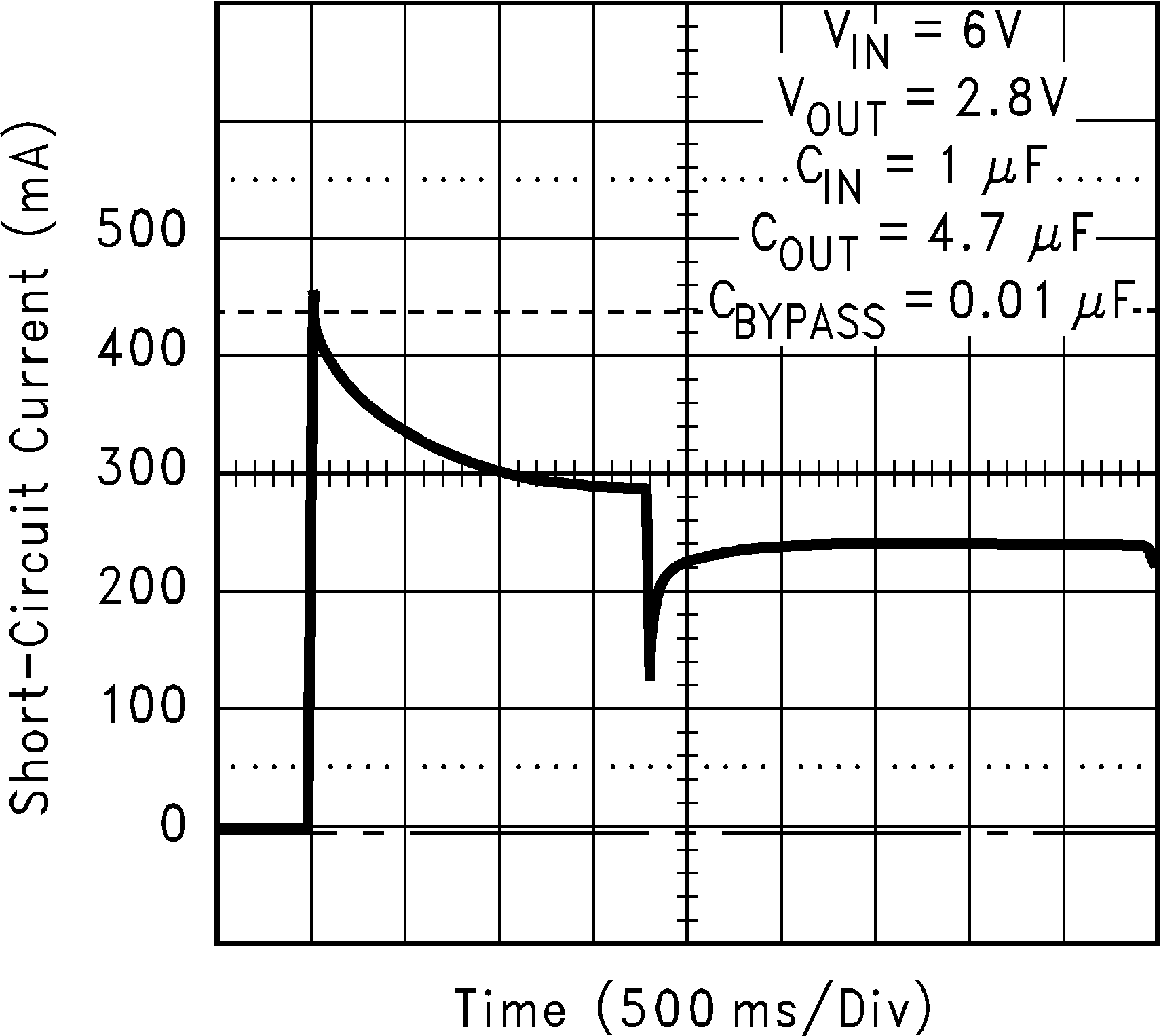 Figure 5-3 Short-Circuit
Current (Legacy Chip)
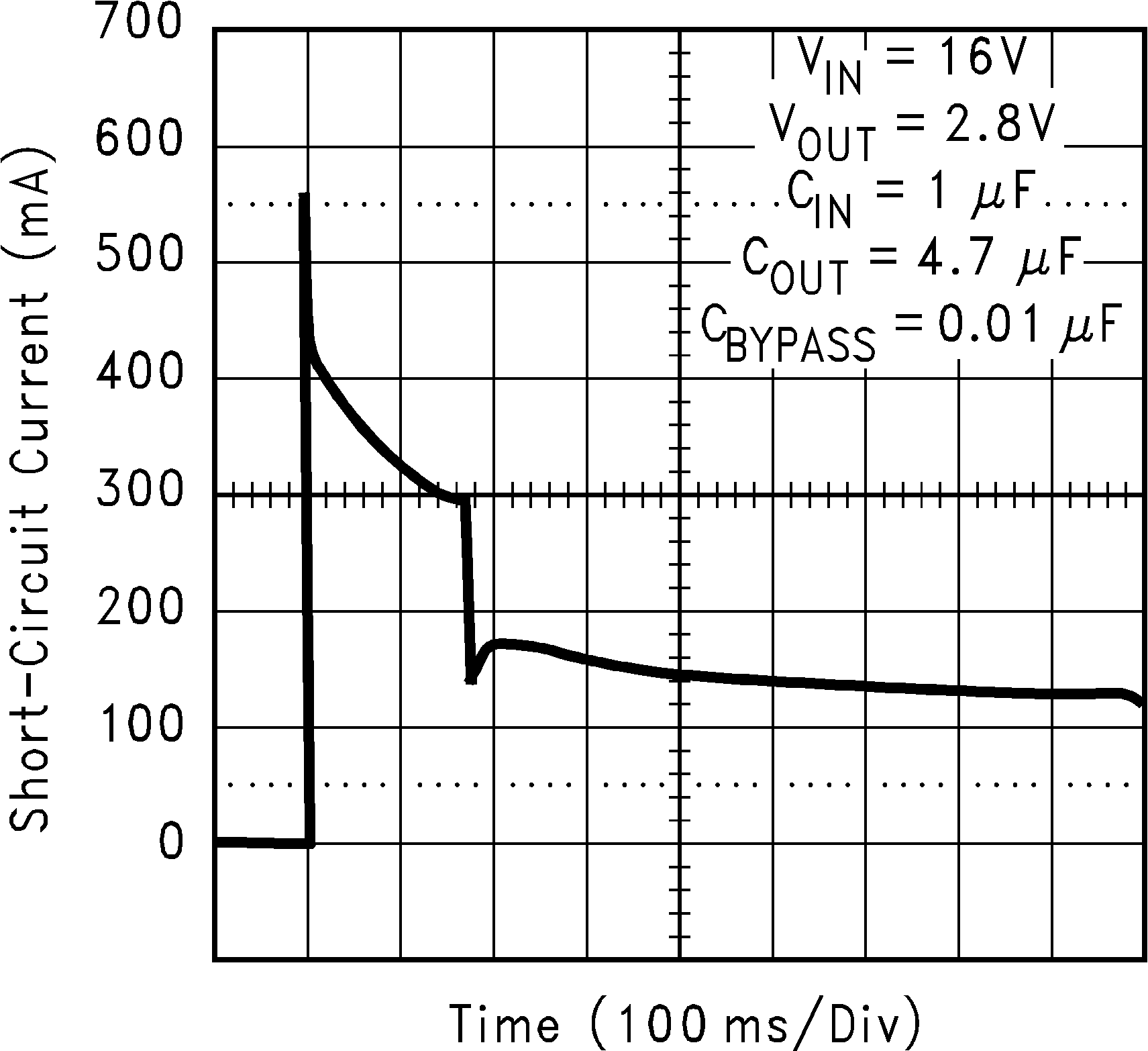 Figure 5-5 Short-Circuit
Current (Legacy Chip)
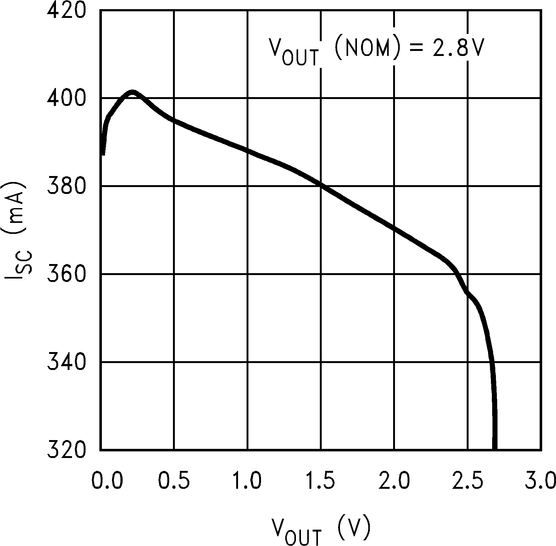 Figure 5-7 Short-Circuit
Current vs Output Voltage (Legacy Chip)
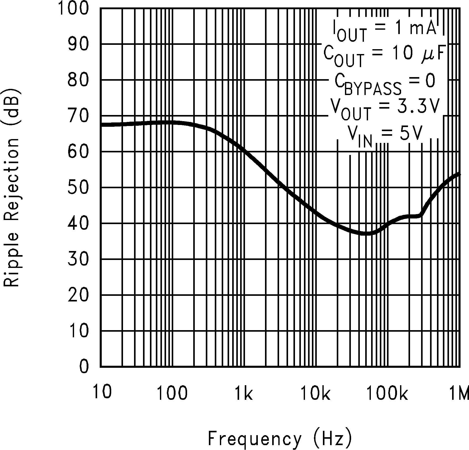
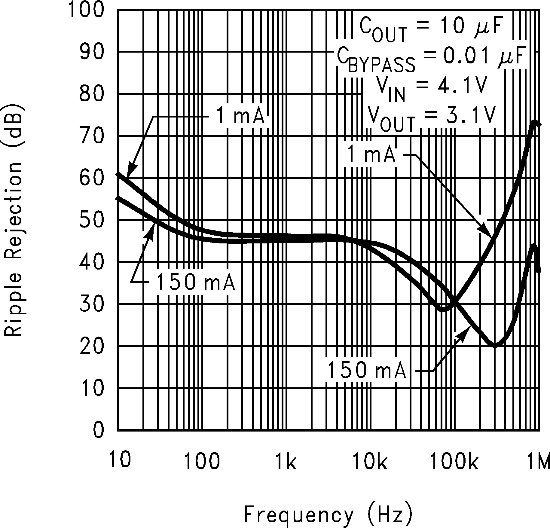 Figure 5-9 Ripple
Rejection vs Frequency (Legacy Chip)
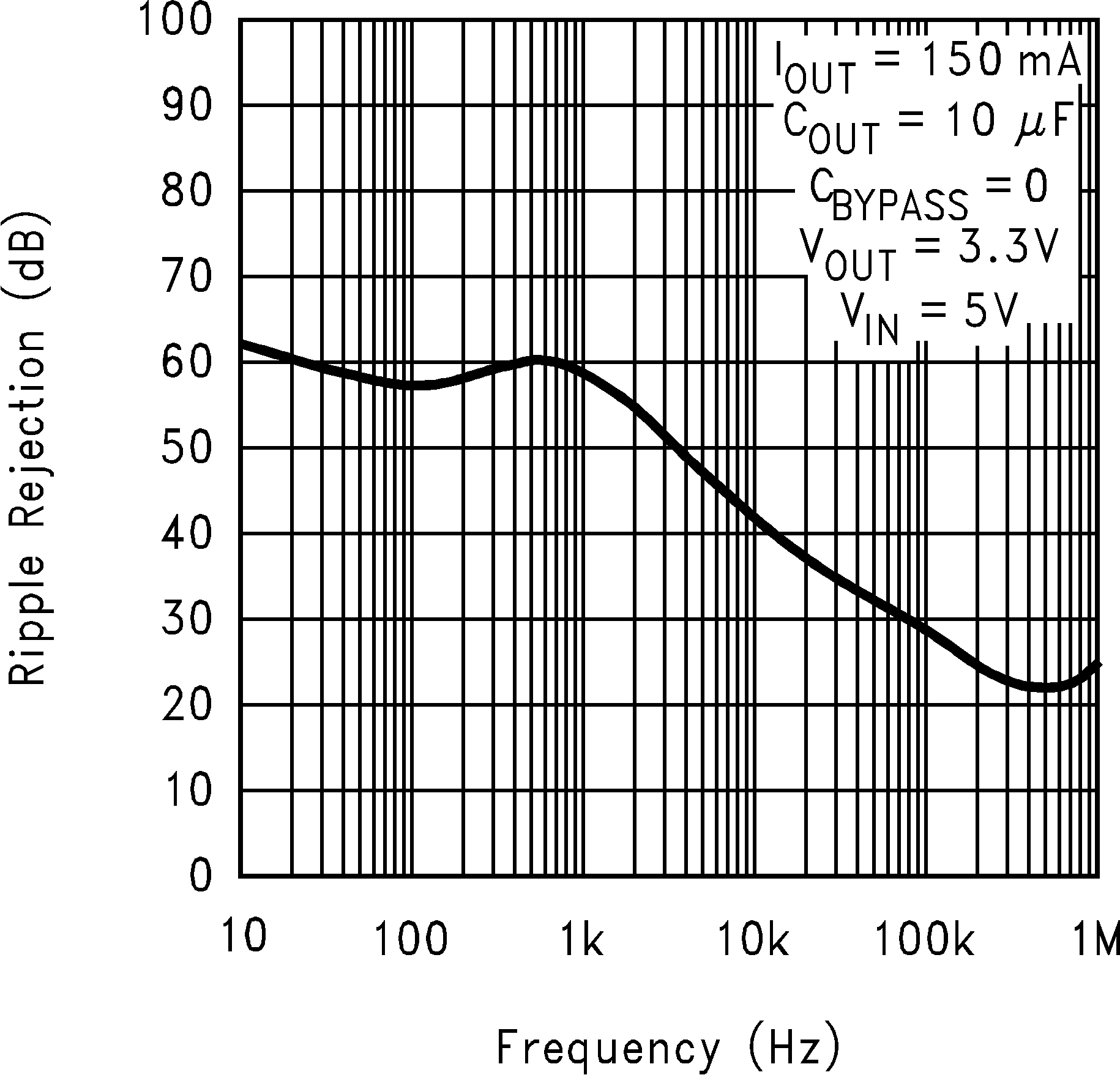
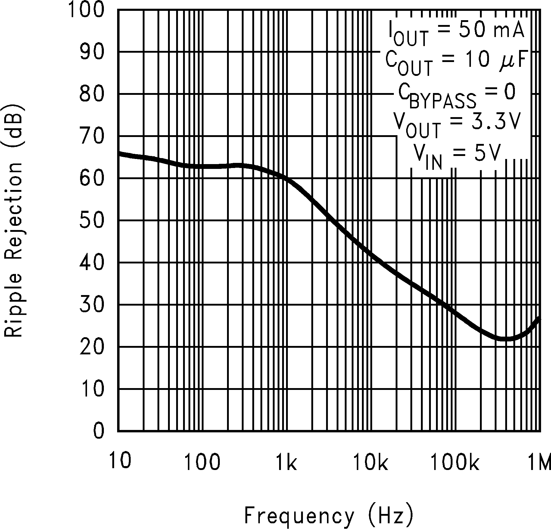 Figure 5-11 Ripple
Rejection vs Frequency (Legacy Chip)
| VIN = 5V, VOUT = 3.3V, COUT = 10μF,
CBYP = 0nF |
Figure 5-13 Ripple Rejection vs Frequency (New
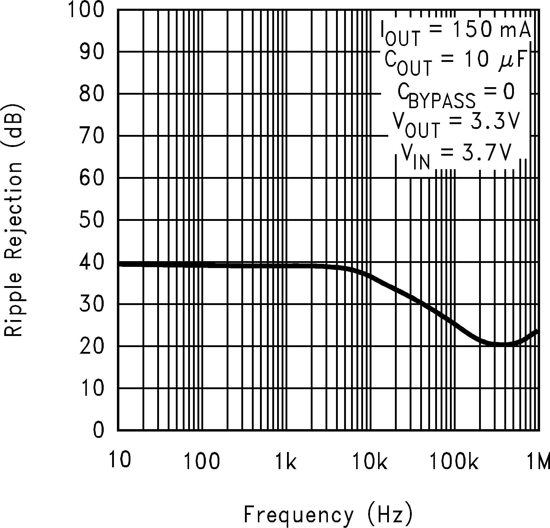
Chip)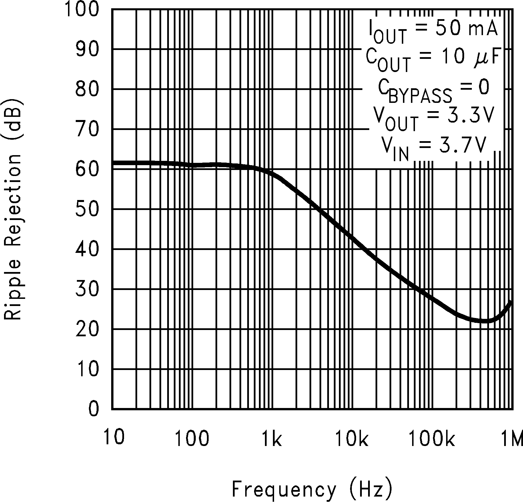 Figure 5-15 Ripple
Rejection vs Frequency (Legacy Chip)
| VIN = 3.7V, VOUT = 3.3V, COUT = 10μF,
CBYP = 0nF |
Figure 5-17 Ripple Rejection vs Frequency (New
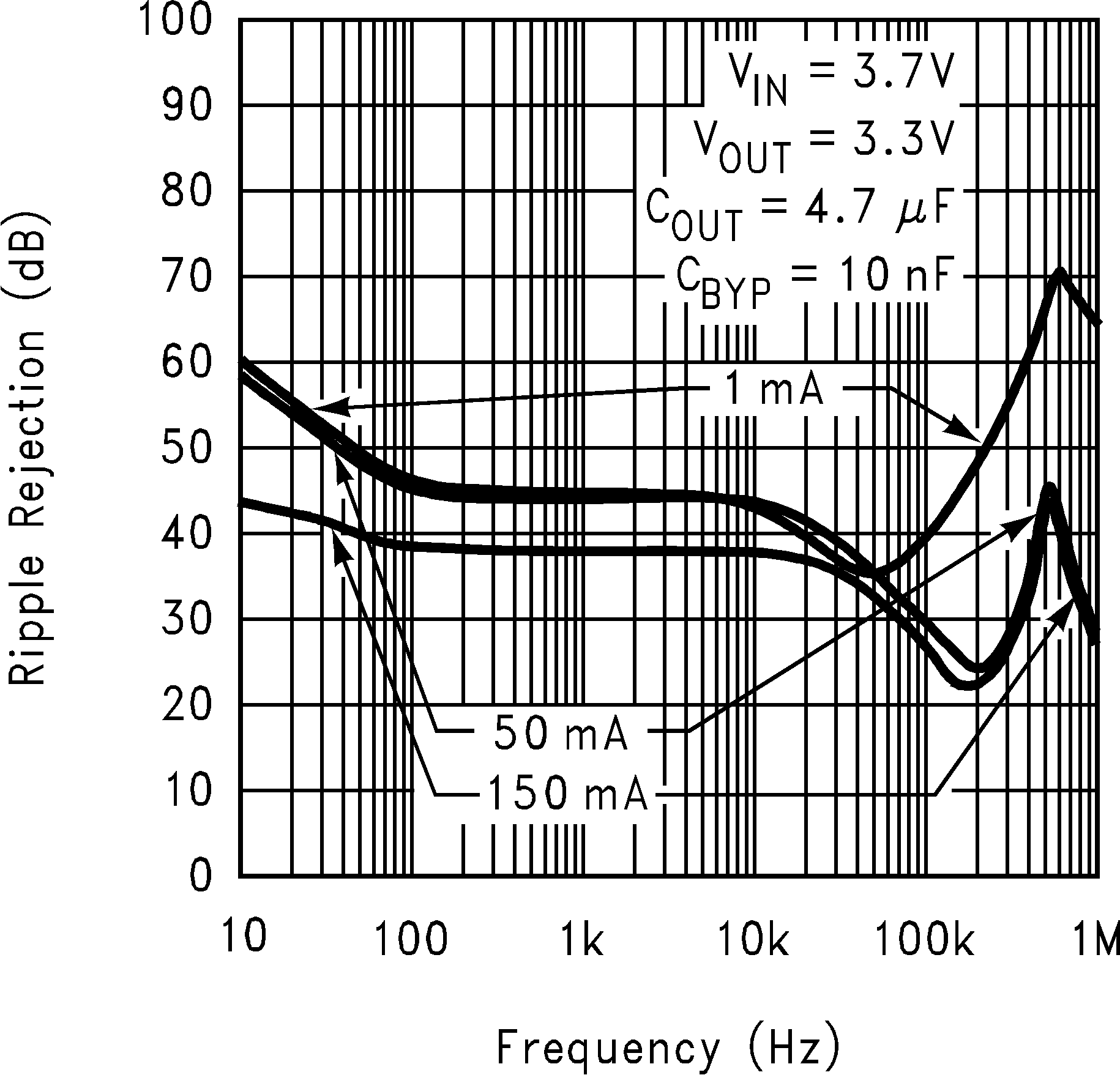
Chip)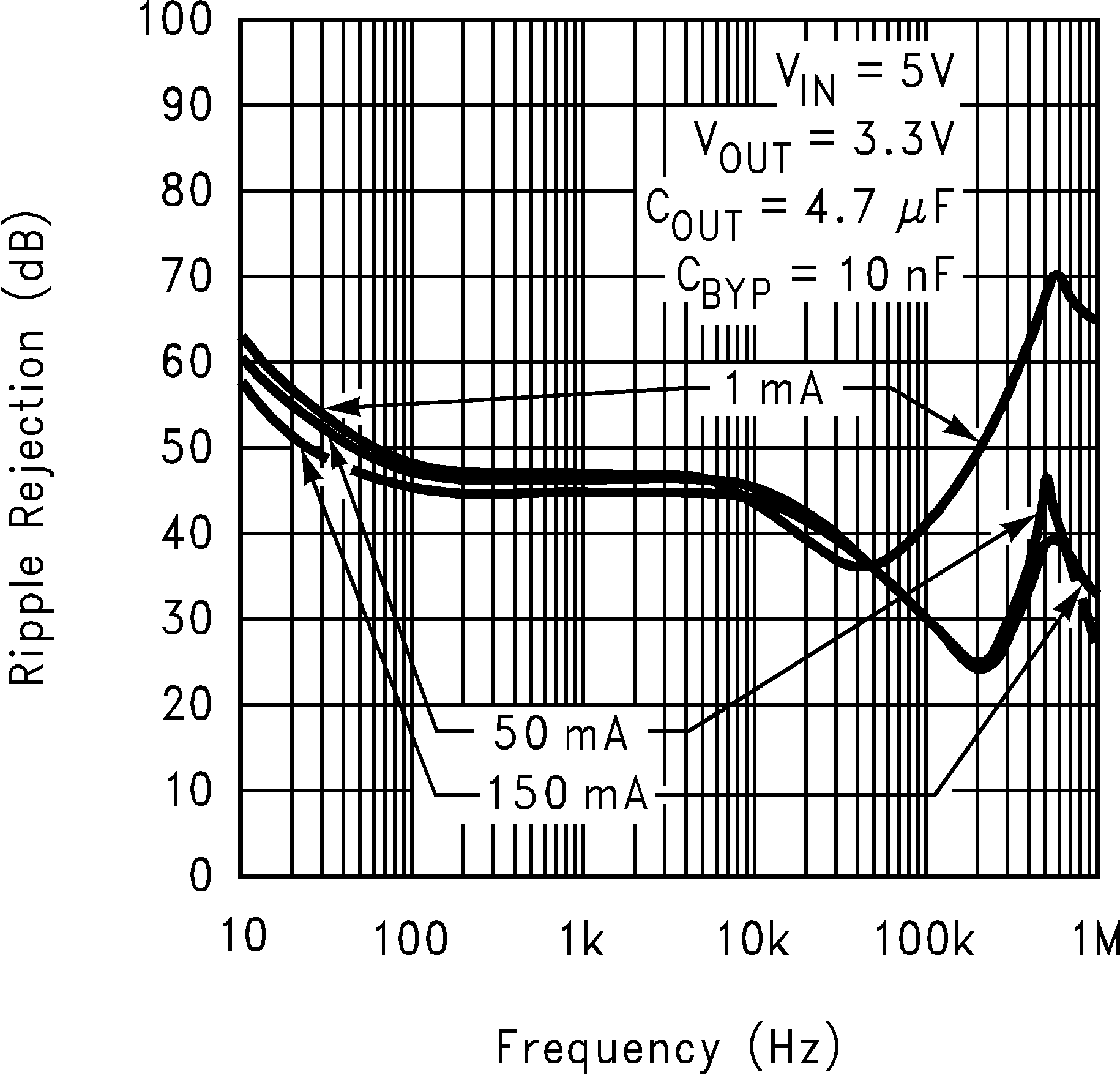 Figure 5-19 Ripple
Rejection vs Frequency (Legacy Chip)
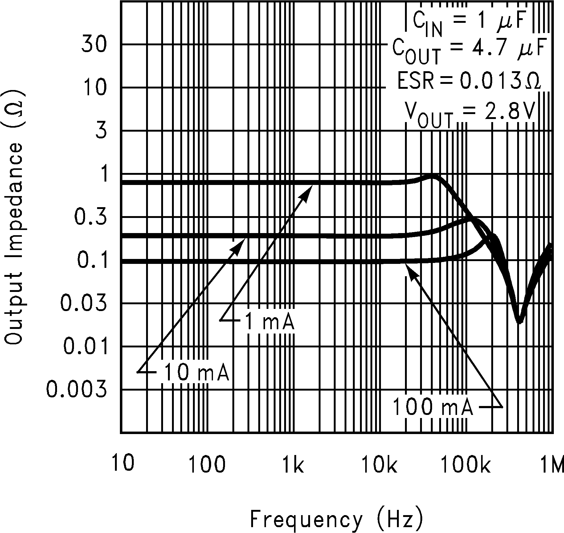
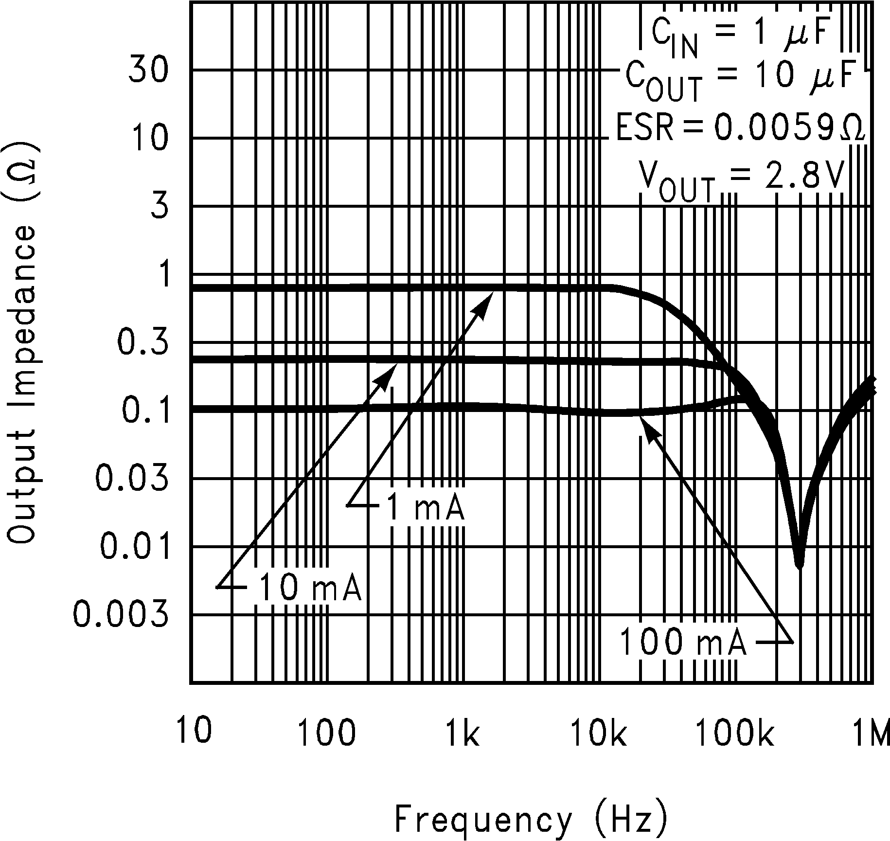 Figure 5-21 Output
Impedance vs Frequency (Legacy Chip)
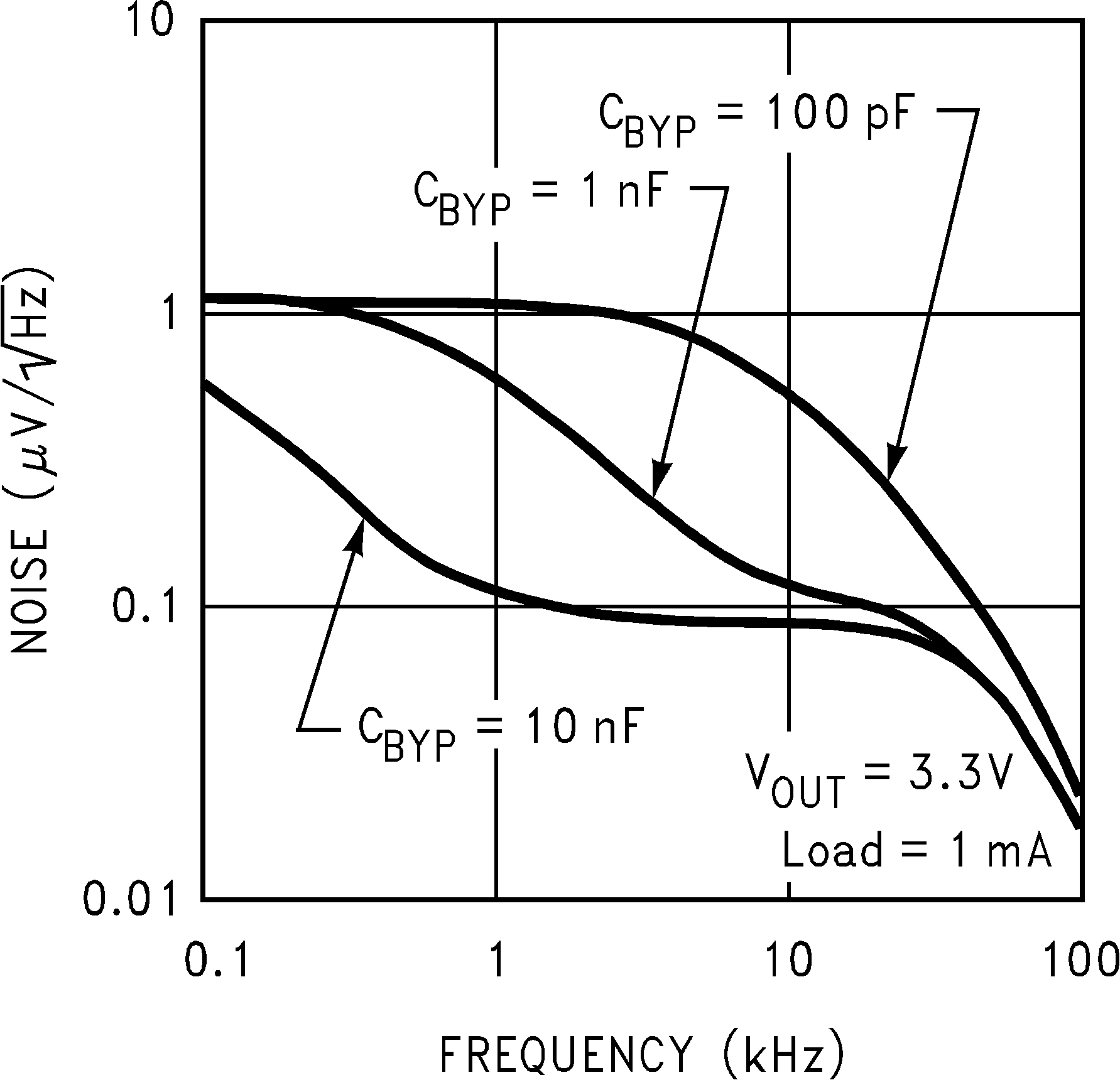 Figure 5-23 Output Noise
Density (Legacy Chip)
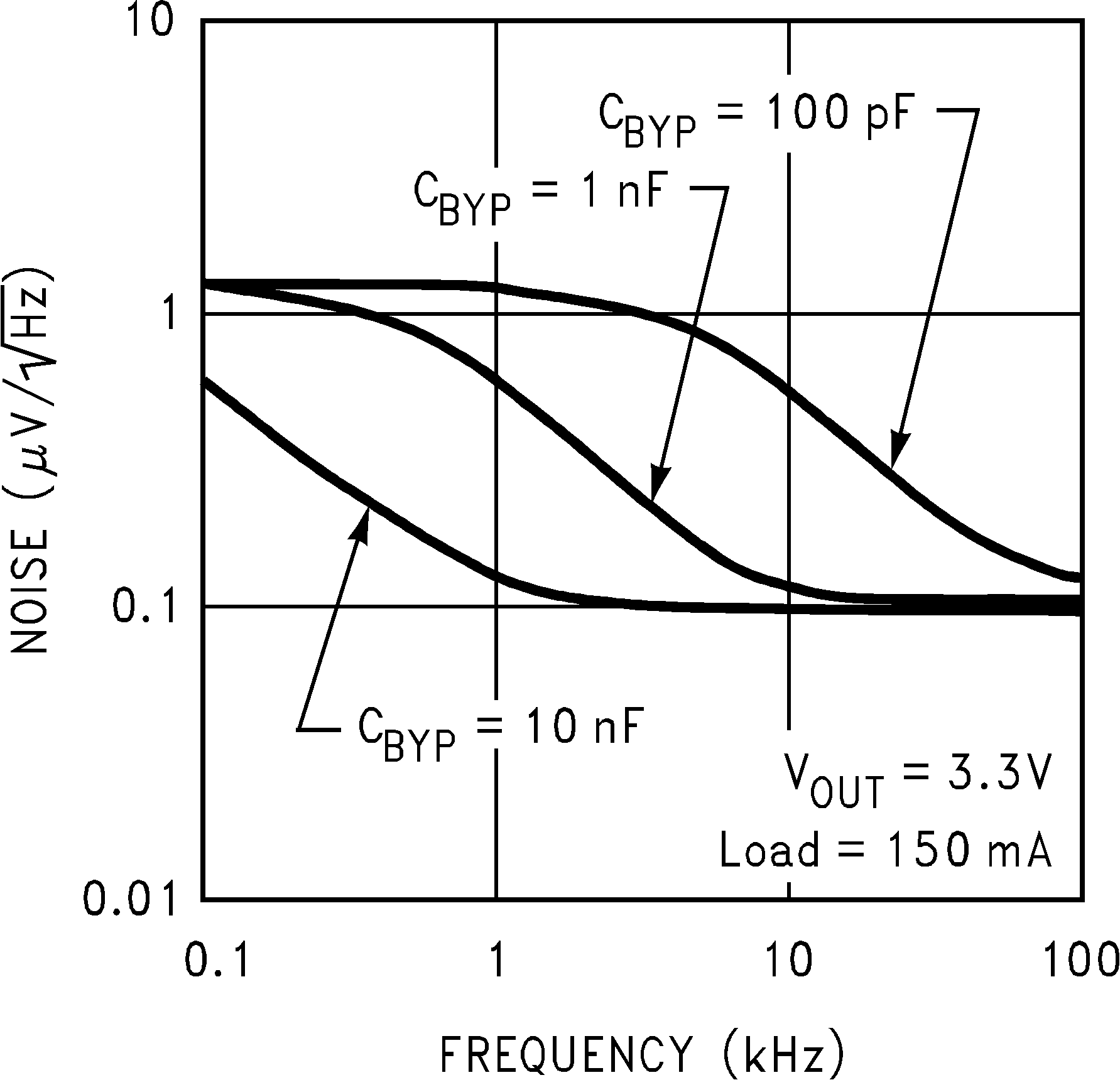 Figure 5-25 Output Noise
Density (Legacy Chip)
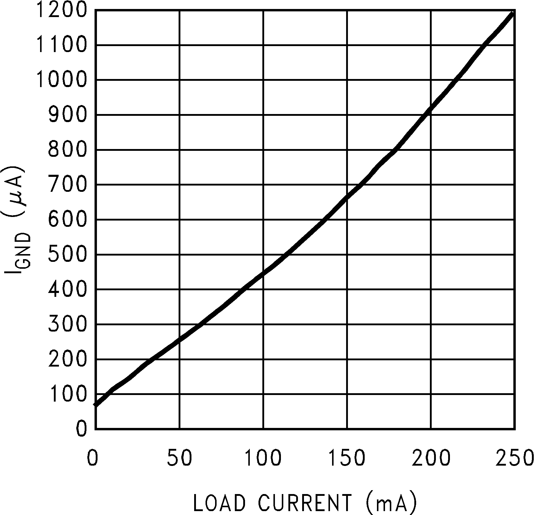 Figure 5-27 GND Pin vs Load
Current (Legacy Chip)
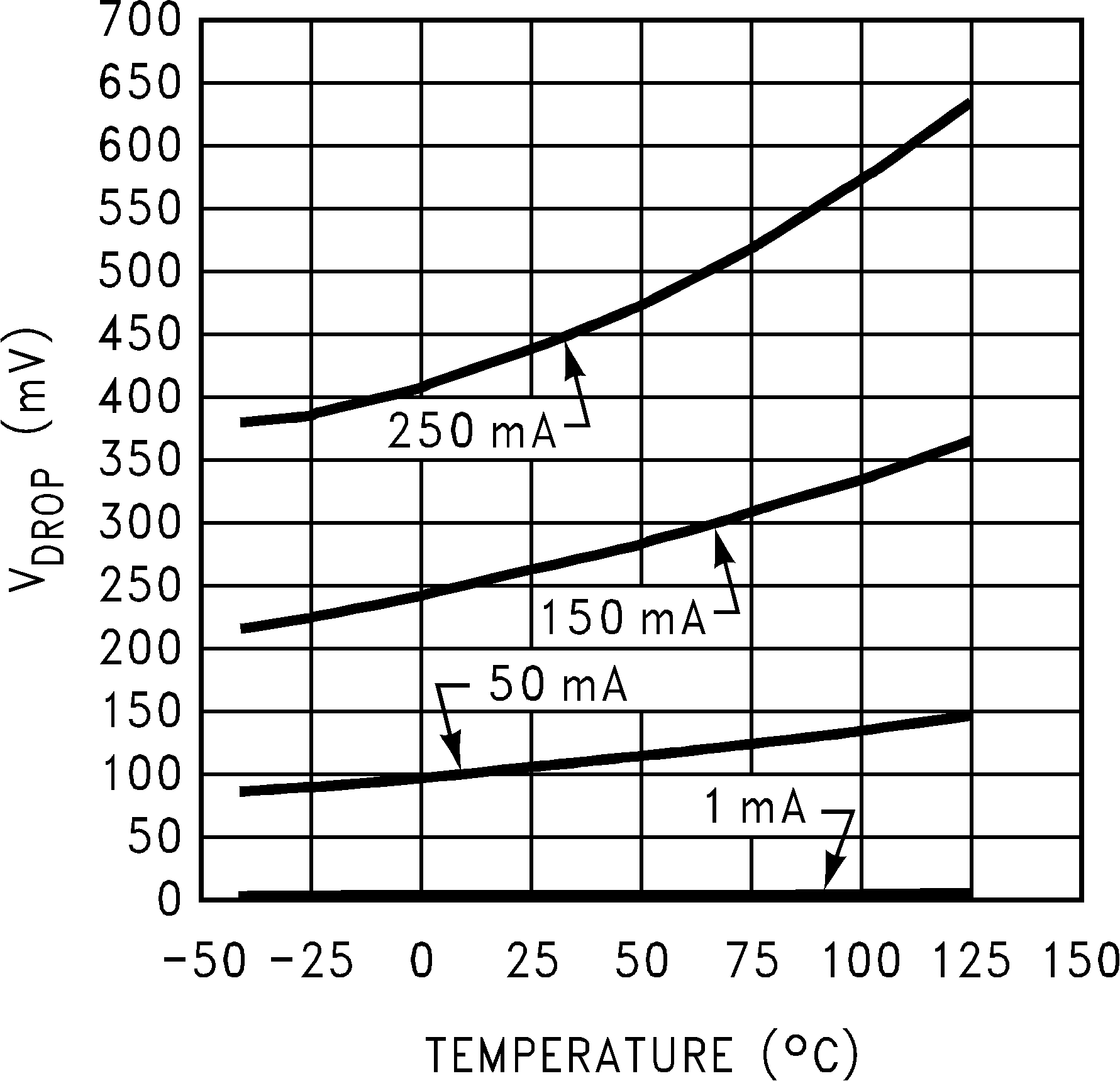 Figure 5-29 Dropout Voltage
vs Temperature (Legacy Chip)
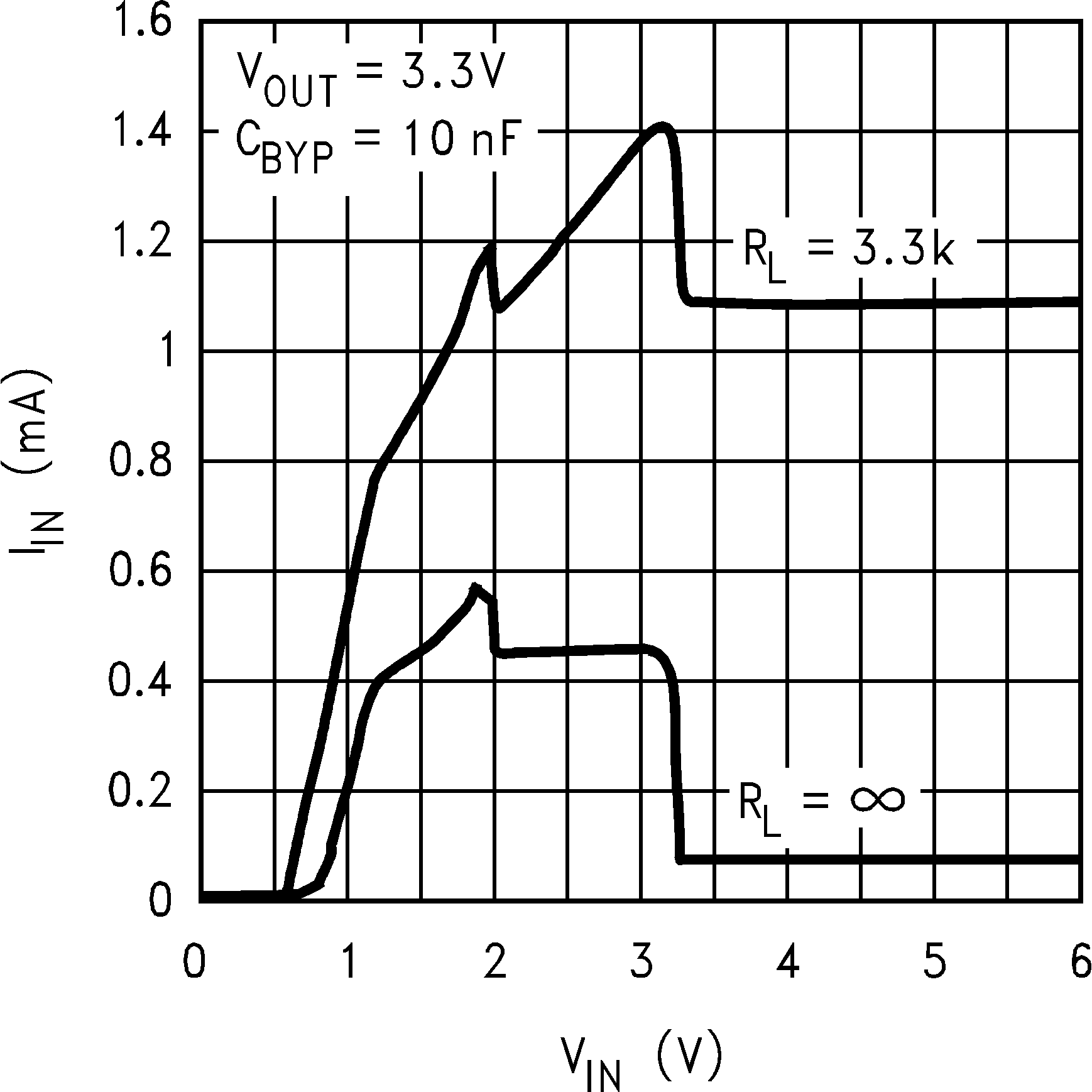 Figure 5-31 Input Current
vs Input Voltage (Legacy Chip)
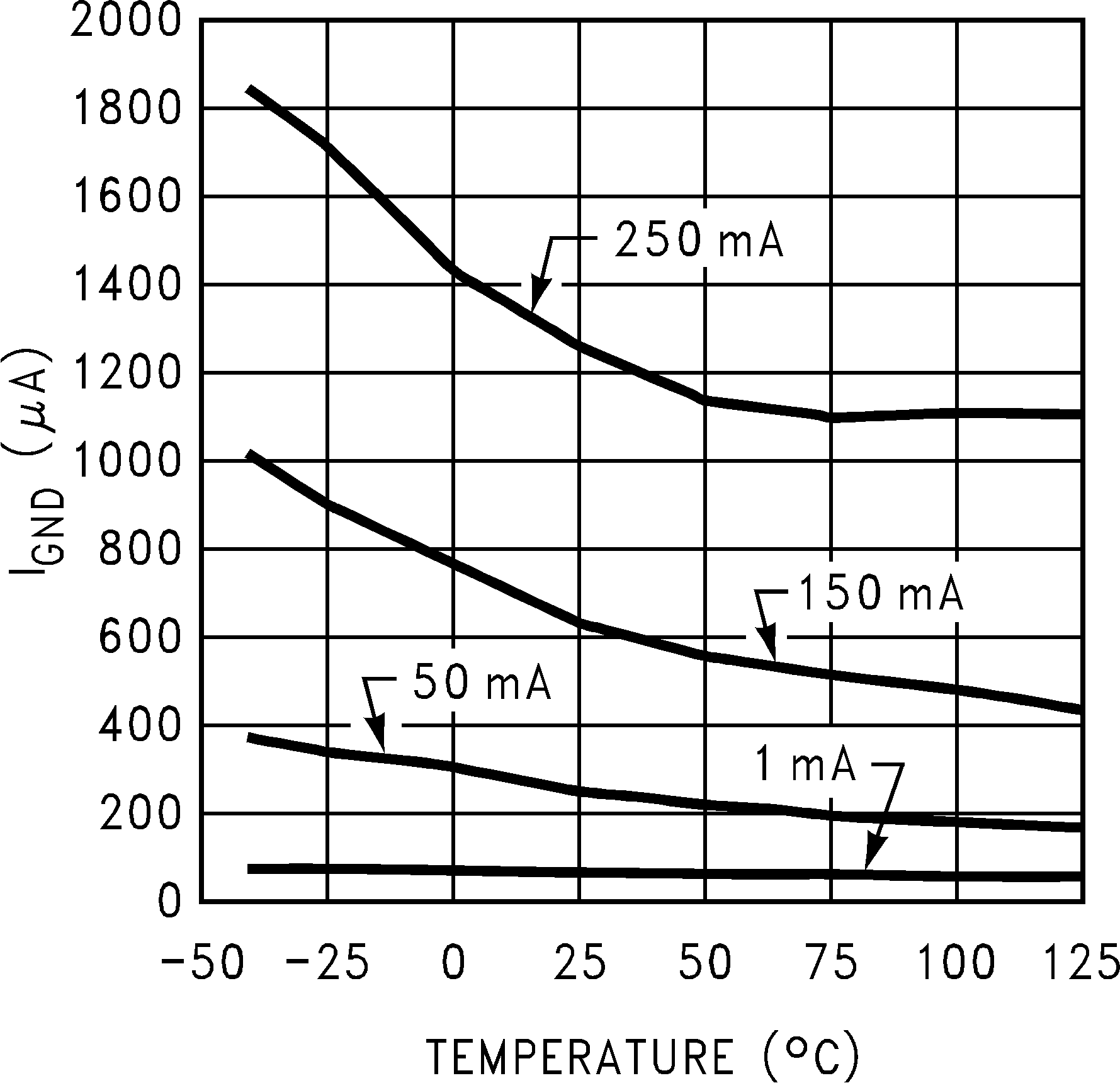 Figure 5-33 IGND
vs Load and Temperature (Legacy Chip)
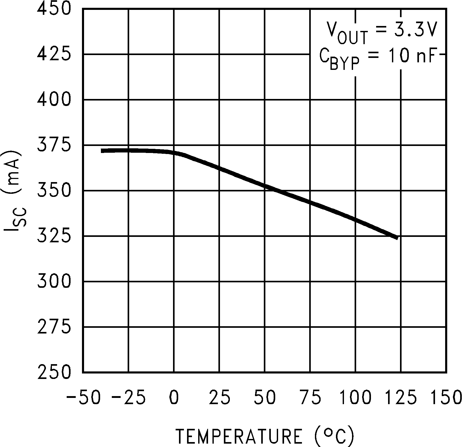 Figure 5-35 Short-Circuit
Current vs Temperature (Legacy Chip)
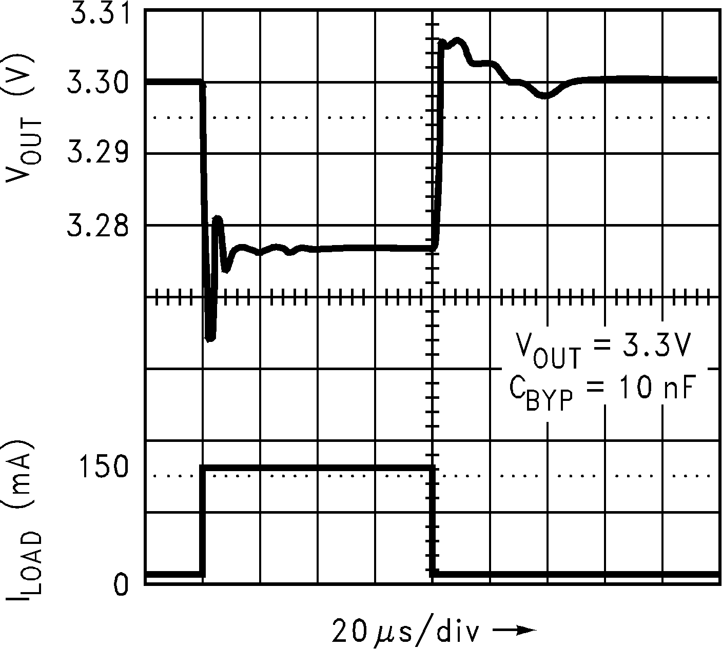 Figure 5-37 Load Transient
Response (Legacy Chip)
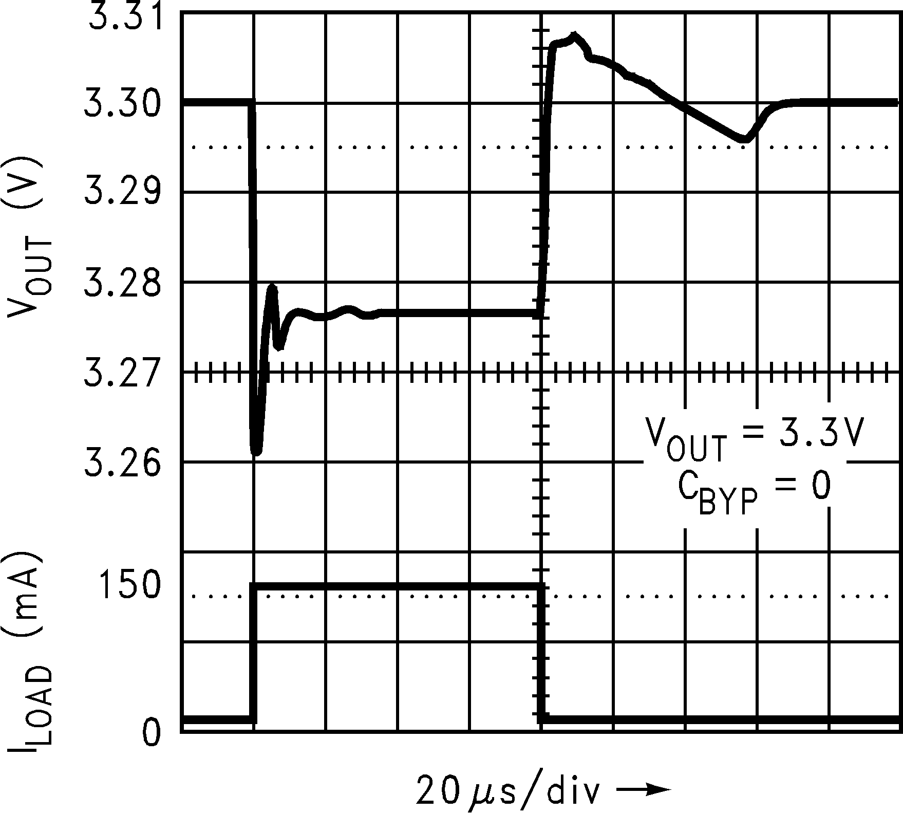 Figure 5-39 Load Transient
Response (Legacy Chip)
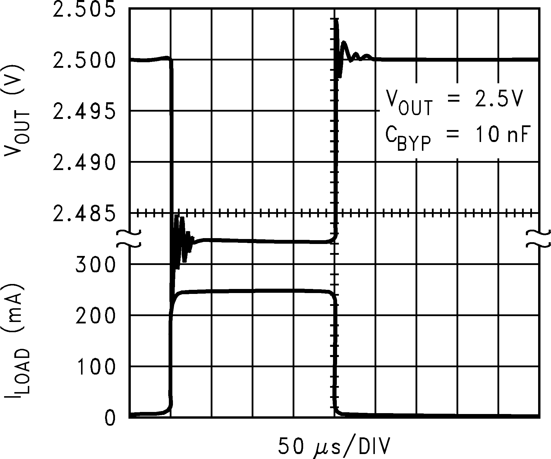 Figure 5-41 Load Transient
Response (Legacy Chip)
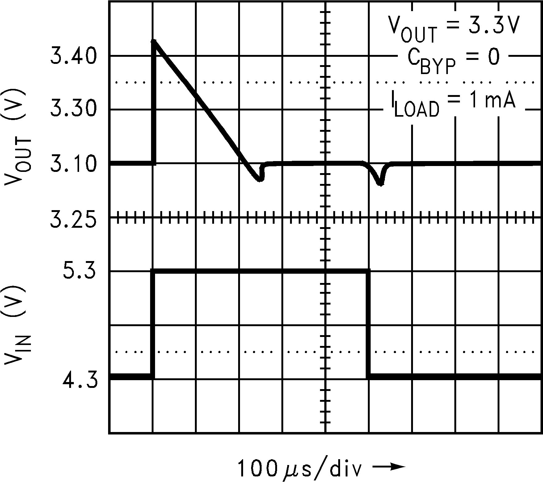 Figure 5-43 Line Transient
Response (Legacy Chip)
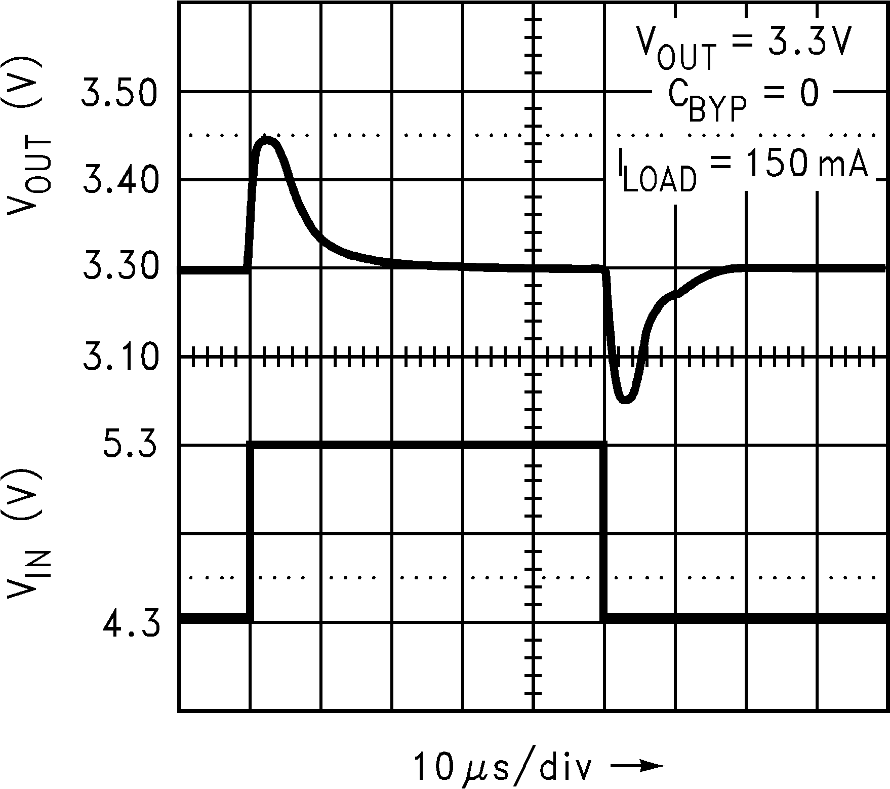 Figure 5-45 Line Transient
Response (Legacy Chip)
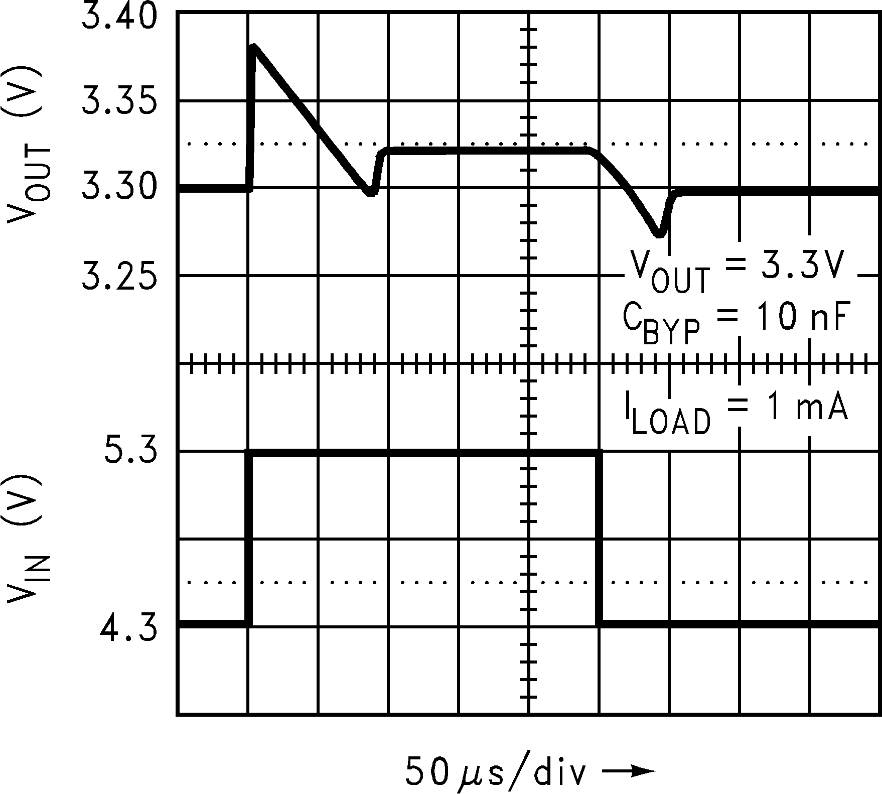 Figure 5-47 Line Transient
Response (Legacy Chip)
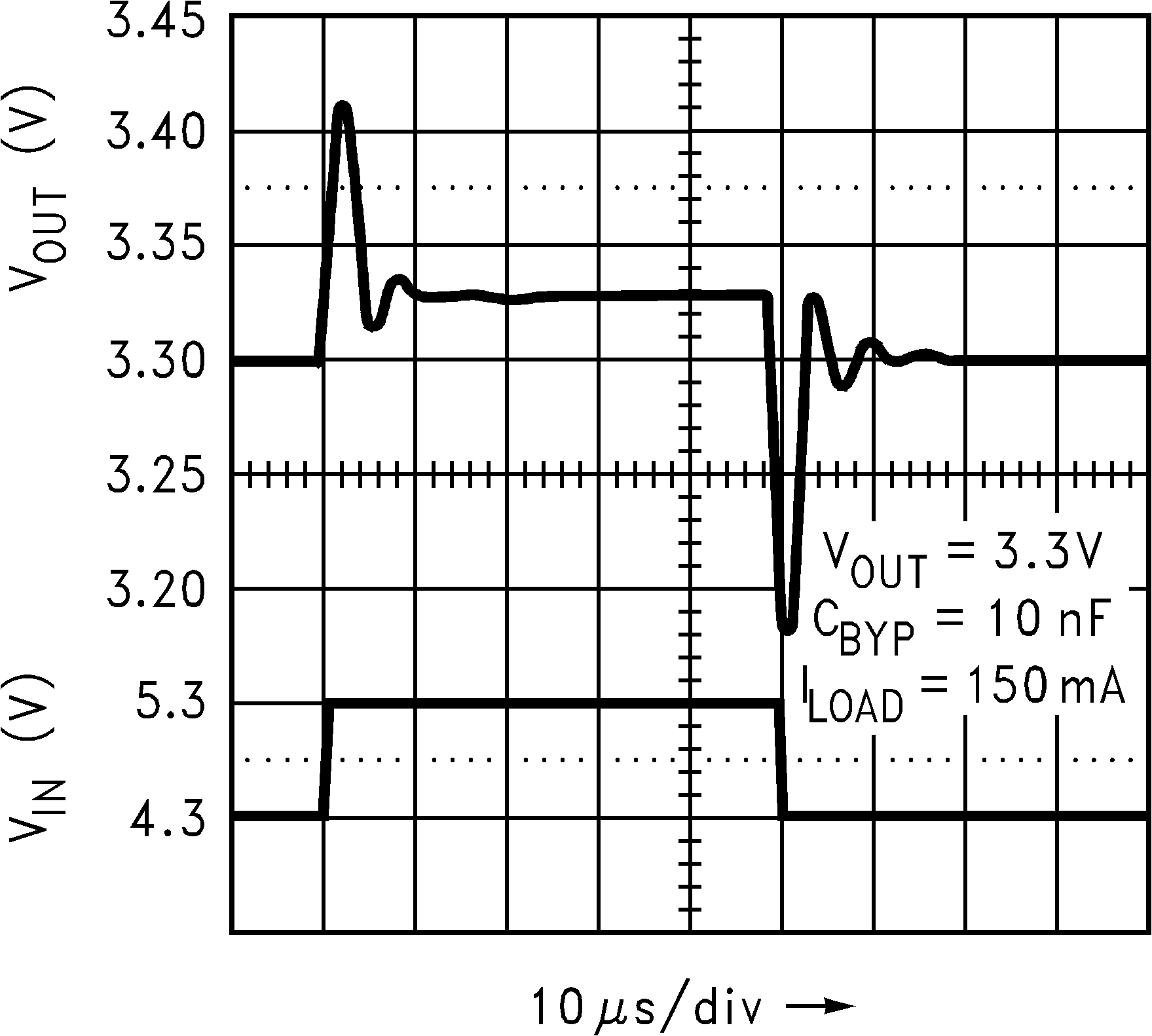 Figure 5-49 Line Transient
Response (Legacy Chip)
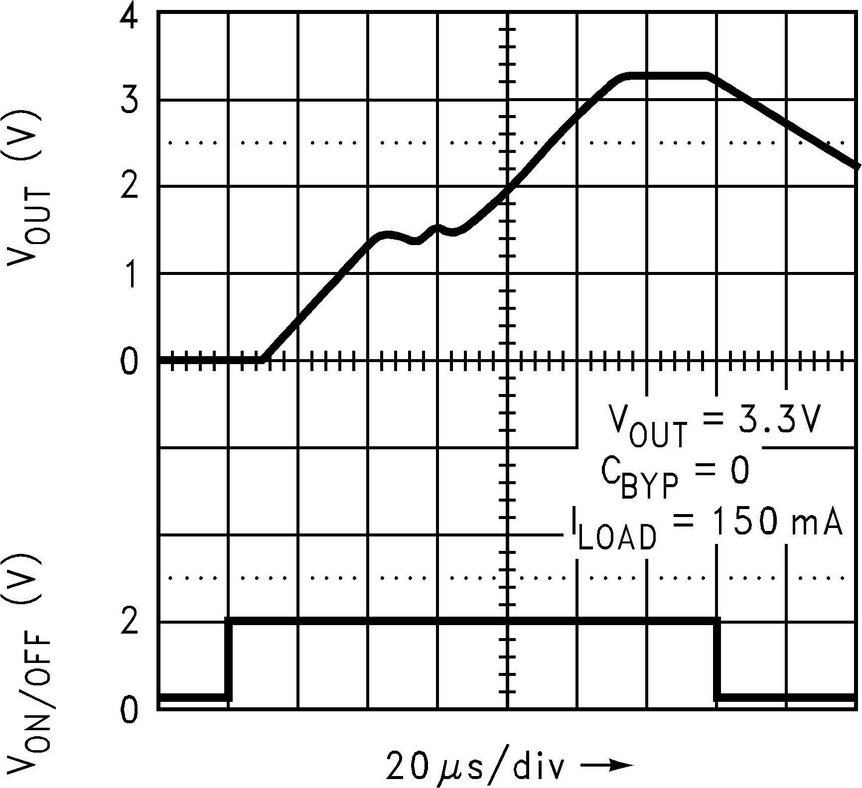 Figure 5-51 Turn-On Time
(Legacy Chip)
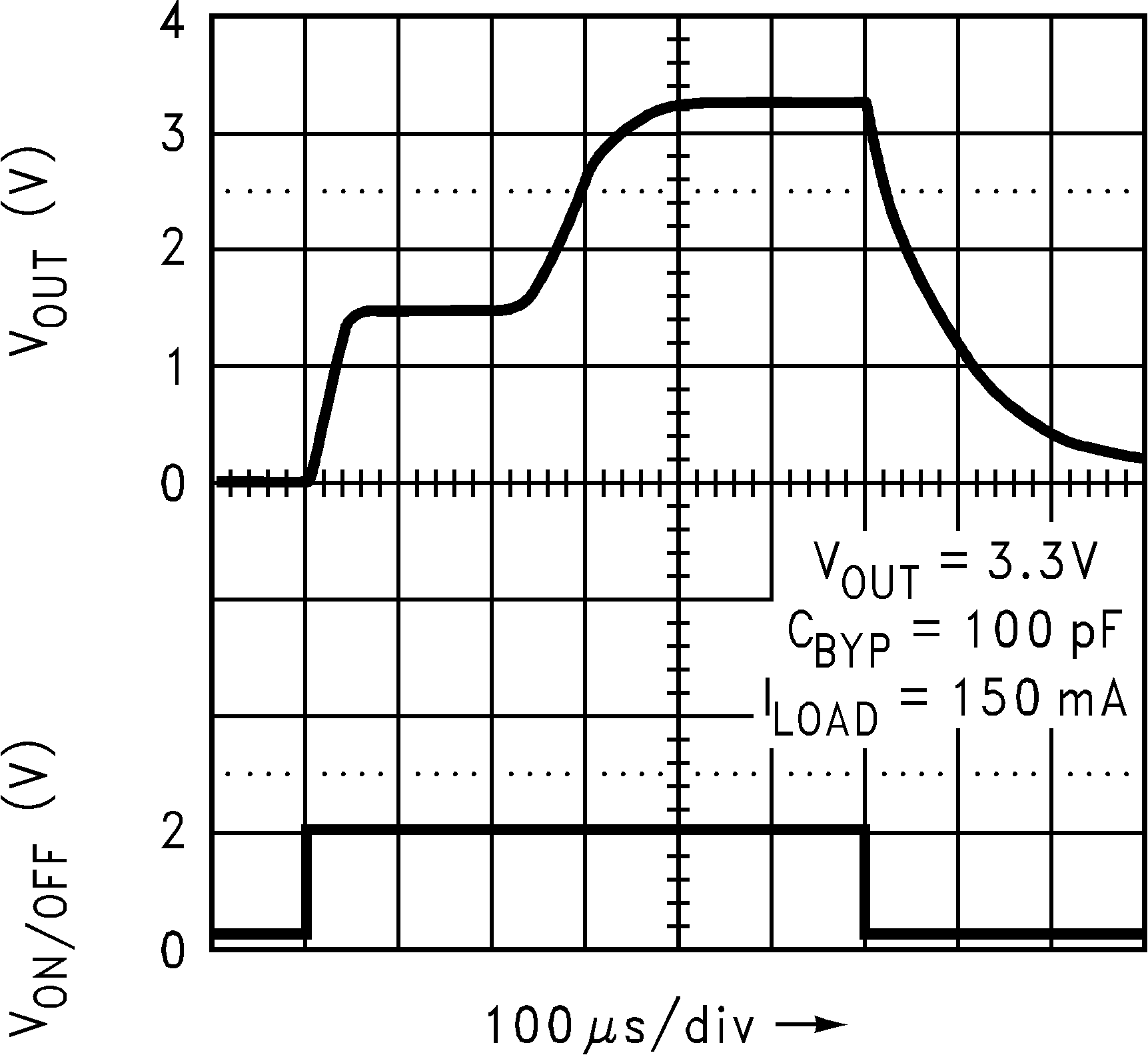 Figure 5-53 Turn-On Time
(Legacy Chip)
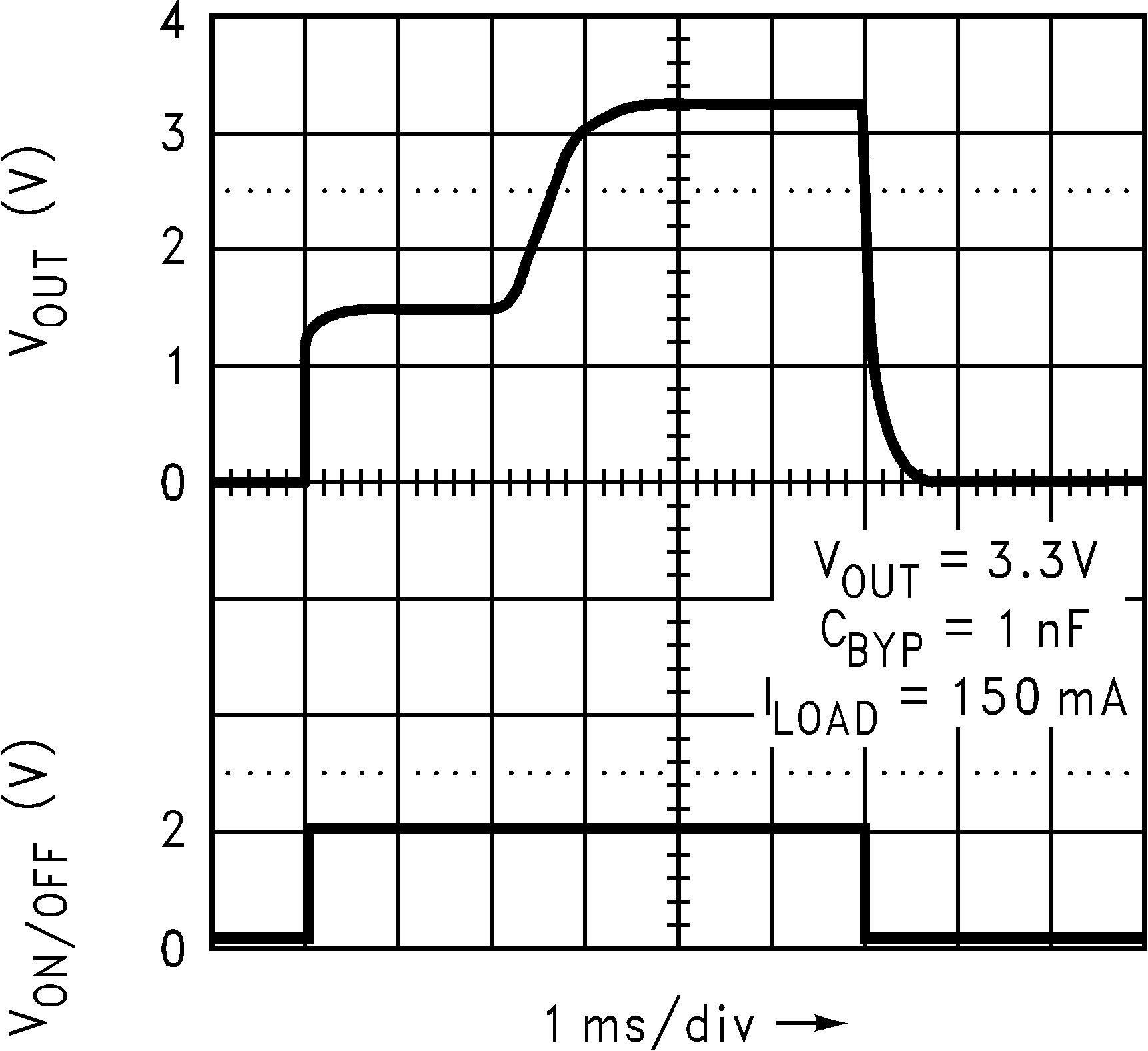 Figure 5-55 Turn-On Time
(Legacy Chip)
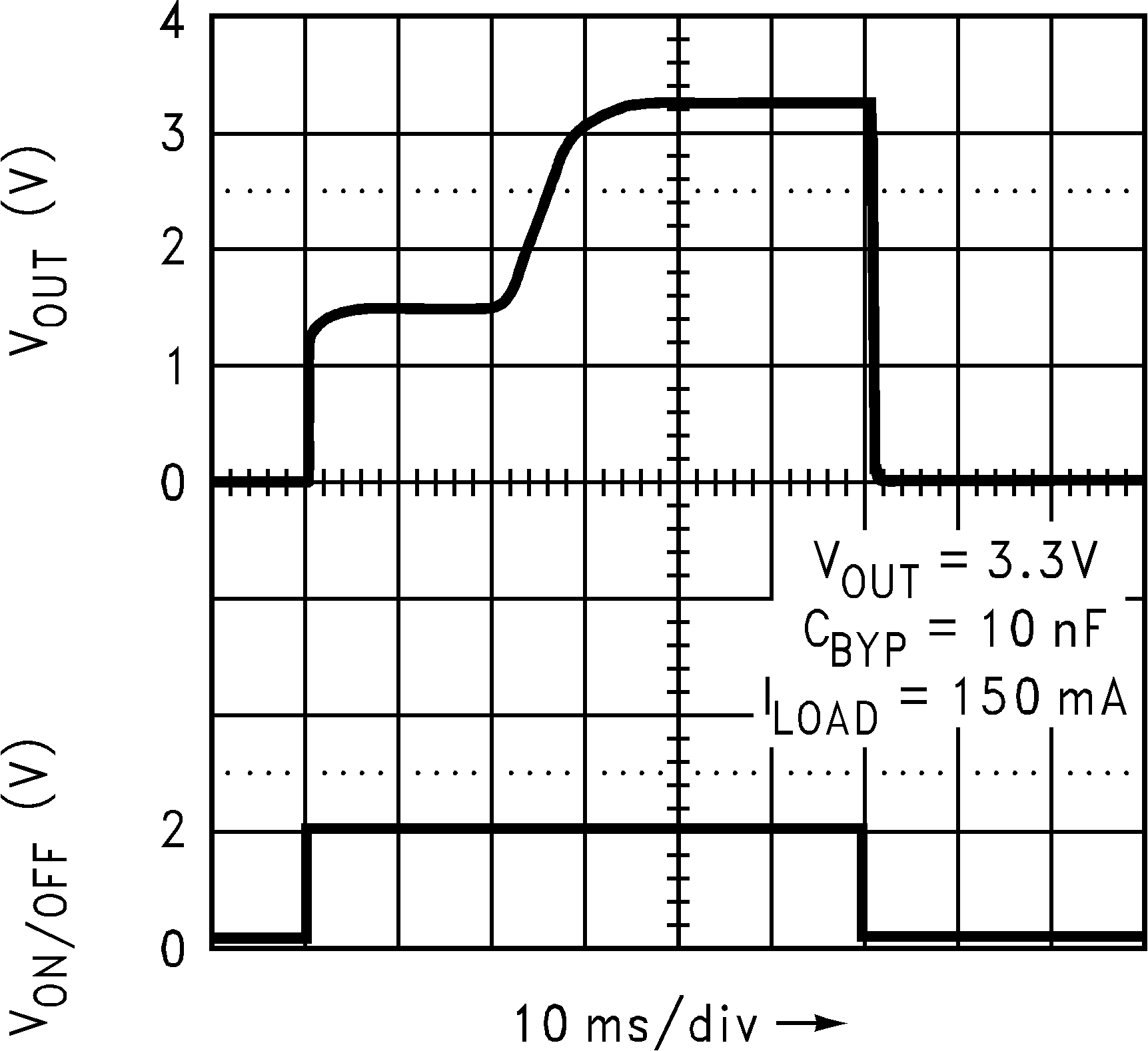 Figure 5-57 Turn-On Time
(Legacy Chip)
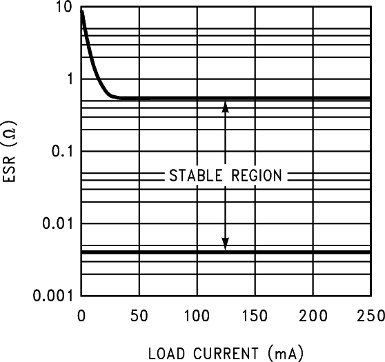 Figure 5-59 Stable ESR Range vs Load Current
(Legacy Chip)
 Figure 5-2 VOUT
vs Temperature (New Chip)
 Figure 5-4 Short-Circuit Current vs Time (New
Chip)
 Figure 5-6 Short-Circuit Current vs Time (New
Chip)
 Figure 5-8 Short-Circuit Current vs Output
Voltage (New Chip)
 Figure 5-10 Ripple
Rejection vs Frequency (Legacy Chip)
 Figure 5-12 Ripple
Rejection vs Frequency (Legacy Chip)
 Figure 5-14 Ripple
Rejection vs Frequency (Legacy Chip)
 Figure 5-16 Ripple
Rejection vs Frequency (Legacy Chip)
 Figure 5-18 Ripple
Rejection vs Frequency (Legacy Chip)
| VIN = 5V, VOUT = 3.3V, COUT = 10μF,
CBYP = 10nF |
Figure 5-20 Ripple Rejection vs Frequency (New
Chip) Figure 5-22 Output
Impedance vs Frequency (Legacy Chip)
 Figure 5-24 Output Noise Density vs Frequency
(New Chip)
| VOUT = 3.3V, IOUT = 150mA |
Figure 5-26 Output Noise Density vs Frequency
(New Chip) Figure 5-28 GND Pin vs Load
Current (New Chip)
 Figure 5-30 Dropout Voltage
vs Temperature (New Chip)
 Figure 5-32 Input Current vs Input Voltage (New
Chip)
 Figure 5-34 IGND
vs Load and Temperature (New Chip)
 Figure 5-36 Short-Circuit Current vs Temperature
(New Chip)
 Figure 5-38 Load Transient (New Chip)
 Figure 5-40 Load Transient Response (New
Chip)
| VOUT = 3.3V, dI/dt = 1A/μs |
Figure 5-42 Load Transient Response (New
Chip)
VOUT = 3.3V, CBYP = 0nF, ΔVIN = 1V,
IOUT = 1mA,
dV/dt = 1V/μs |
Figure 5-44 Line Transient Response (New
Chip)
VOUT = 3.3V, CBYP = 0nF, ΔVIN = 1V,
IOUT = 150mA,
dV/dt = 1V/μs |
Figure 5-46 Line Transient Response (New
Chip)
VOUT = 3.3V, CBYP = 10nF, ΔVIN = 1V,
IOUT = 1mA,
dV/dt = 1V/μs |
Figure 5-48 Line Transient Response (New
Chip)
| VOUT = 3.3V, CBYP = 10nF, ΔVIN = 1V,
IOUT = 150mA, dV/dt = 1V/μs |
Figure 5-50 Line Transient Response (New
Chip) Figure 5-52 Turn-On Time (New Chip)
 Figure 5-54 Turn-On Time (New Chip)
 Figure 5-56 Turn-On Time (New Chip)
 Figure 5-58 Turn-On Time (New Chip)


 Figure 5-59 Stable ESR Range vs Load Current
(Legacy Chip)


