SNVSBF5C July   2019  – May 2020 LP3470A

PRODUCTION DATA.  

  1. Features
  2. Applications
  3. Description
    1.     Device Images
      1.      Basic Operating Circuit
      2.      Typical Supply Current for LP3470A
  4. Revision History
  5. Device Comparison Table
  6. Pin Configuration and Functions
    1.     Pin Functions
  7. Specifications
    1. 7.1 Absolute Maximum Ratings
    2. 7.2 ESD Ratings
    3. 7.3 Recommended Operating Conditions
    4. 7.4 Thermal Information
    5. 7.5 Electrical Characteristics
    6. 7.6 Timing Requirements
    7. 7.7 Typical Characteristics
  8. Detailed Description
    1. 8.1 Overview
    2. 8.2 Functional Block Diagram
    3. 8.3 Feature Description
      1. 8.3.1 RESET Time-Out Period
      2. 8.3.2 RESET Output
      3. 8.3.3 Pull-up Resistor Selection
      4. 8.3.4 VCC Transient Immunity
    4. 8.4 Device Functional Modes
      1. 8.4.1 RESET Output Low
      2. 8.4.2 RESET Output High
  9. Application and Implementation
    1. 9.1 Application Information
    2. 9.2 Typical Application
      1. 9.2.1 Design Requirements
      2. 9.2.2 Detailed Design Procedure
      3. 9.2.3 Application Curves
  10. 10Power Supply Recommendations
  11. 11Layout
    1. 11.1 Layout Guidelines
    2. 11.2 Layout Example
  12. 12Device and Documentation Support
    1. 12.1 Receiving Notification of Documentation Updates
    2. 12.2 Support Resources
    3. 12.3 Trademarks
    4. 12.4 Electrostatic Discharge Caution
    5. 12.5 Glossary
  13. 13Mechanical, Packaging, and Orderable Information

Package Options

Mechanical Data (Package|Pins)
Thermal pad, mechanical data (Package|Pins)
Orderable Information

Application Curves

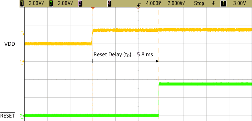
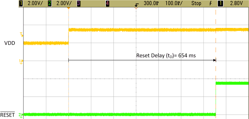
Two capacitor values for CSRT (0.01 µF and 1 µF) are used as examples to show the programmability of the output time delay as shown in Figure 12 and Figure 13.

LP3470A TPS3840_reset_delay_cap_0p01uF.gif
Figure 12. Reset Delay Time with 0.01-µF Capacitor at SRT
LP3470A TPS3840_reset_delay_cap_1uF.gif
Figure 13. Reset Delay Time with 1-µF Capacitor at SRT