SNVS522I August 2007 – August 2015 LP38501-ADJ , LP38503-ADJ
PRODUCTION DATA.
- 1 Features
- 2 Applications
- 3 Description
- 4 Revision History
- 5 Pin Configurations and Functions
- 6 Specifications
- 7 Detailed Description
- 8 Application and Implementation
- 9 Power Supply Recommendations
- 10Layout
- 11Device and Documentation Support
- 12Mechanical, Packaging, and Orderable Information
Package Options
Mechanical Data (Package|Pins)
Thermal pad, mechanical data (Package|Pins)
- KTT|5
Orderable Information
8 Application and Implementation
NOTE
Information in the following applications sections is not part of the TI component specification, and TI does not warrant its accuracy or completeness. TI’s customers are responsible for determining suitability of components for their purposes. Customers should validate and test their design implementation to confirm system functionality.
8.1 Application Information
The LP38501-ADJ and LP38503-ADJ devices can provide 3-A output current with 2.7-V to 5.5-V input voltage. These ultra-low-dropout linear regulators respond very quickly to step changes in load, making them suitable for low-voltage microprocessor applications. Input and output capacitors of at least 10 µF are required.
8.2 Typical Applications
8.2.1 Design Requirements
For LP3850x-ADJ typical applications, use the parameters listed in Table 1 as the input parameters.
Table 1. Design Parameters
| DESIGN PARAMETERS | VALUE |
|---|---|
| Input voltage | 2.7 V to 5.5 V |
| Output voltage | 0.6 V to 5 V (adjustable) |
| Output current | 3 A (maximum) |
| Input capacitor | 10 µF (minimum) |
| Output capacitor | 10 µF (minimum) |
8.2.2 Detailed Design Procedure
8.2.2.1 External Capacitors
The LP38501-ADJ and LP38503-ADJ require that at least 10-µF (±20%) capacitors be used at the input and output pins located within one cm of the device. Larger capacitors may be used without limit on size for both CIN and COUT. Capacitor tolerances such as temperature variation and voltage loading effects must be considered when selecting capacitors to ensure that they provide the minimum required amount of capacitance under all operating conditions for the application.
In general, ceramic capacitors are best for noise bypassing and transient response because of their ultra low ESR. It must be noted that if ceramics are used, only the types with X5R or X7R dielectric ratings must be used (never Z5U or Y5F). Capacitors which have the Z5U or Y5F characteristics have a drop in capacitance of as much as 50% if their temperature increases from 25°C to 85°C. In addition, the capacitance drops significantly with applied voltage: a typical Z5U or Y5F capacitor can lose as much as 60% of its rated capacitance if only half of the rated voltage is applied to it. For these reasons, only X5R and X7R ceramics must be used.
8.2.2.2 Input Capacitor
All linear regulators can be affected by the source impedance of the voltage which is connected to the input. If the source impedance is too high, the reactive component of the source may affect the control loop’s phase margin. To ensure proper loop operation, the ESR of the capacitor used for CIN must not exceed 0.5 Ω. Any good quality ceramic capacitor meets this requirement, as well as many good quality tantalums. Aluminum electrolytic capacitors may also work, but can possibly have an ESR which increases significantly at cold temperatures. If the ESR of the input capacitor may exceed 0.5 Ω, it is recommended that a 2.2-µF ceramic capacitor be used in parallel, as this assures stable loop operation.
8.2.2.3 Output Capacitor
Any type of capacitor may be used for COUT, with no limitations on minimum or maximum ESR, as long as the minimum amount of capacitance is present. The amount of capacitance can be increased without limit. Increasing the size of COUT typically gives improved load transient response.
8.2.2.4 Setting The Output Voltage
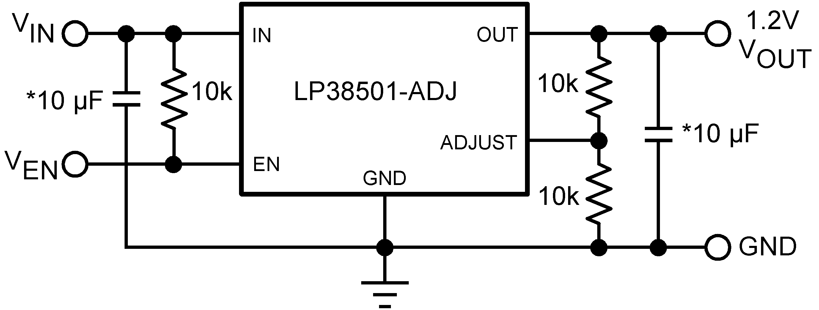
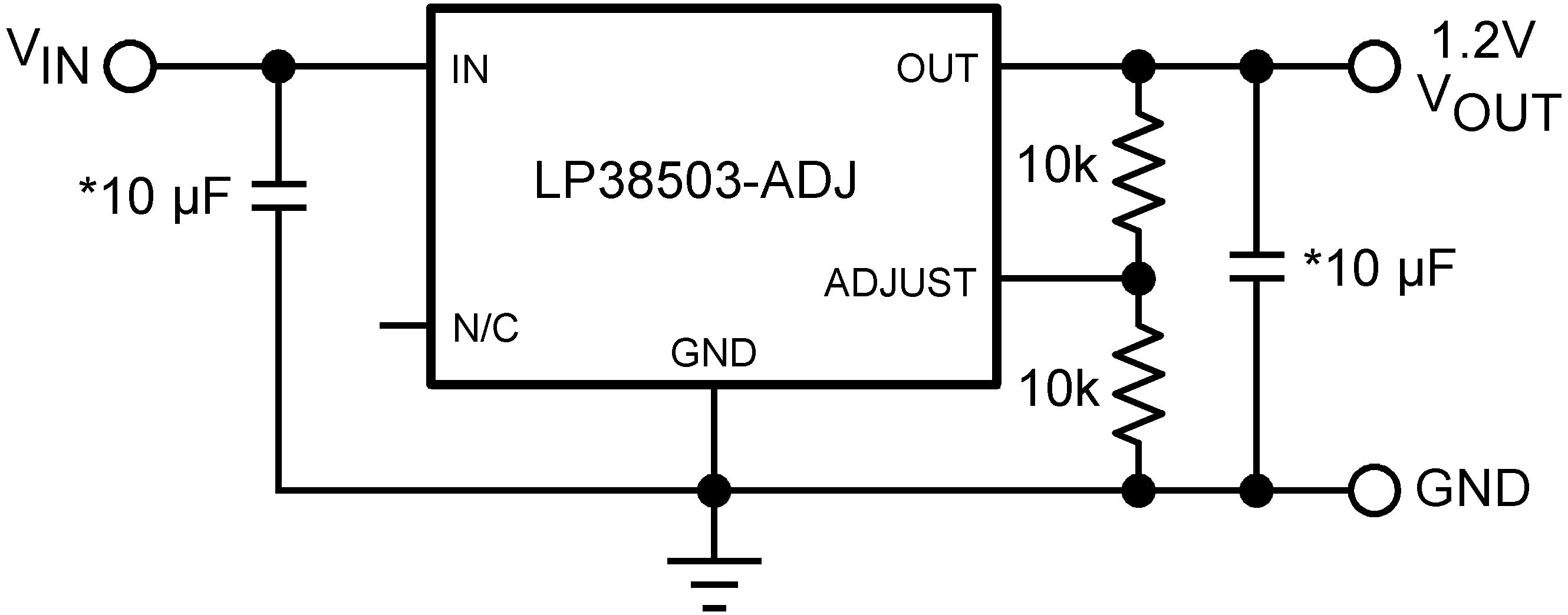
The output voltage of the LP38501-ADJ and LP38503-ADJ can be set to any value between 0.6 V and 5 V using two external resistors shown as R1 and R2 in Figure 25.
 Figure 25. Setting Output Voltage
The value of R2 must always be less than or equal to 10 kΩ for good loop compensation. R1 can be selected for a given VOUT using the following formula:
where
- VADJ is the adjust pin voltage
- IADJ is the bias current flowing into the adjust pin
8.2.2.5 RFI/EMI Susceptibility
Radio frequency interference (RFI) and electro-magnetic interference (EMI) can degrade any integrated circuit's performance because of the small dimensions of the geometries inside the device. In applications where circuit sources are present which generate signals with significant high frequency energy content (> 1 MHz), care must be taken to ensure that this does not affect the device regulator.
If RFI/EMI noise is present on the input side of the regulator (such as applications where the input source comes from the output of a switching regulator), good ceramic bypass capacitors must be used at the input pin of the device to reduce the amount of EMI conducted into the device.
If the LP38501-ADJ or LP38503-ADJ output is connected to a load which switches at high speed (such as a clock), the high-frequency current pulses required by the load must be supplied by the capacitors on the device output. Because the bandwidth of the regulator loop is less than 300 kHz, the control circuitry cannot respond to load changes above that frequency. This means the effective output impedance of the device at frequencies above 300 kHz is determined only by the output capacitor(s). Ceramic capacitors provide the best performance in this type of application.
In applications where the load is switching at high speed, the output of the device may need RF isolation from the load. In such cases, it is recommended that some inductance be placed between the output capacitor and the load, and good RF bypass capacitors be placed directly across the load. PCB layout is also critical in high noise environments, because RFI/EMI is easily radiated directly into PC traces. Noisy circuitry must be isolated from clean circuits where possible, and grounded through a separate path. At MHz frequencies, ground planes begin to look inductive and RFI/EMI can cause ground bounce across the ground plane. In multi-layer PC Board applications, care must be taken in layout so that noisy power and ground planes do not radiate directly into adjacent layers which carry analog power and ground.
8.2.2.6 Output Noise
Noise is specified in two ways:
- Spot noise or output noise density is the RMS sum of all noise sources, measured at the regulator output, at a specific frequency (measured with a 1-Hz bandwidth). This type of noise is usually plotted on a curve as a function of frequency.
- Total output noise or broadband noise is the RMS sum of spot noise over a specified bandwidth, usually several decades of frequencies.
Spot noise is measured in units µV/√Hz or nV/√Hz and total output noise is measured in µV(RMS). The primary source of noise in low-dropout regulators is the internal reference. In CMOS regulators, noise has a low-frequency component and a high frequency component, which depend strongly on the silicon area and quiescent current.
Noise can generally be reduced in two ways: by increasing the transistor area or increasing the reference current. However, enlarging the transistors increases die size, and increasing the reference current means higher total supply current (GND pin current).
8.2.2.7 Power Dissipation/Heatsinking
The maximum power dissipation (PD(MAX)) of the LP38501-ADJ and LP38503-ADJ is limited by the maximum junction temperature of 125°C, along with the maximum ambient temperature (TA(MAX)) of the application, and the thermal resistance (RθJA) of the package. Under all possible conditions, the junction temperature (TJ) must be within the range specified in the Recommended Operating Conditions. The total power dissipation of the device is given by:
where
- IGND is the operating ground current of the device (specified under Electrical Characteristics).
The maximum allowable junction temperature rise (ΔTJ) depends on the maximum expected ambient temperature (TA(MAX)) of the application, and the maximum allowable junction temperature (TJ(MAX)):
The maximum allowable value for junction-to-ambient thermal resistance, RθJA, can be calculated using the formula:
The LP38501-ADJ and LP38503-ADJ are available in the DDPAK/TO-263 and TO-263 packages. The thermal resistance depends on the amount of copper area allocated to heat transfer.
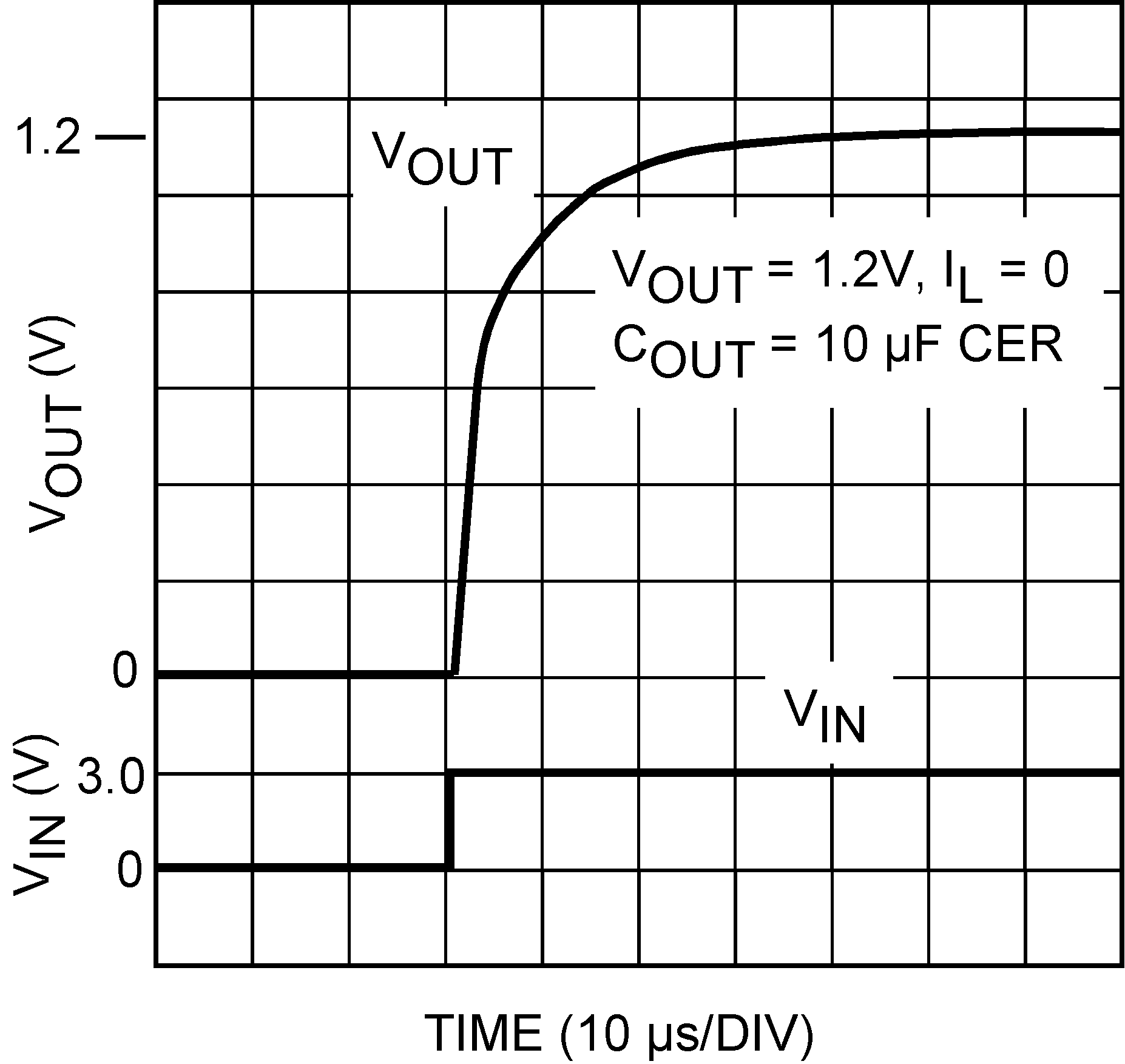
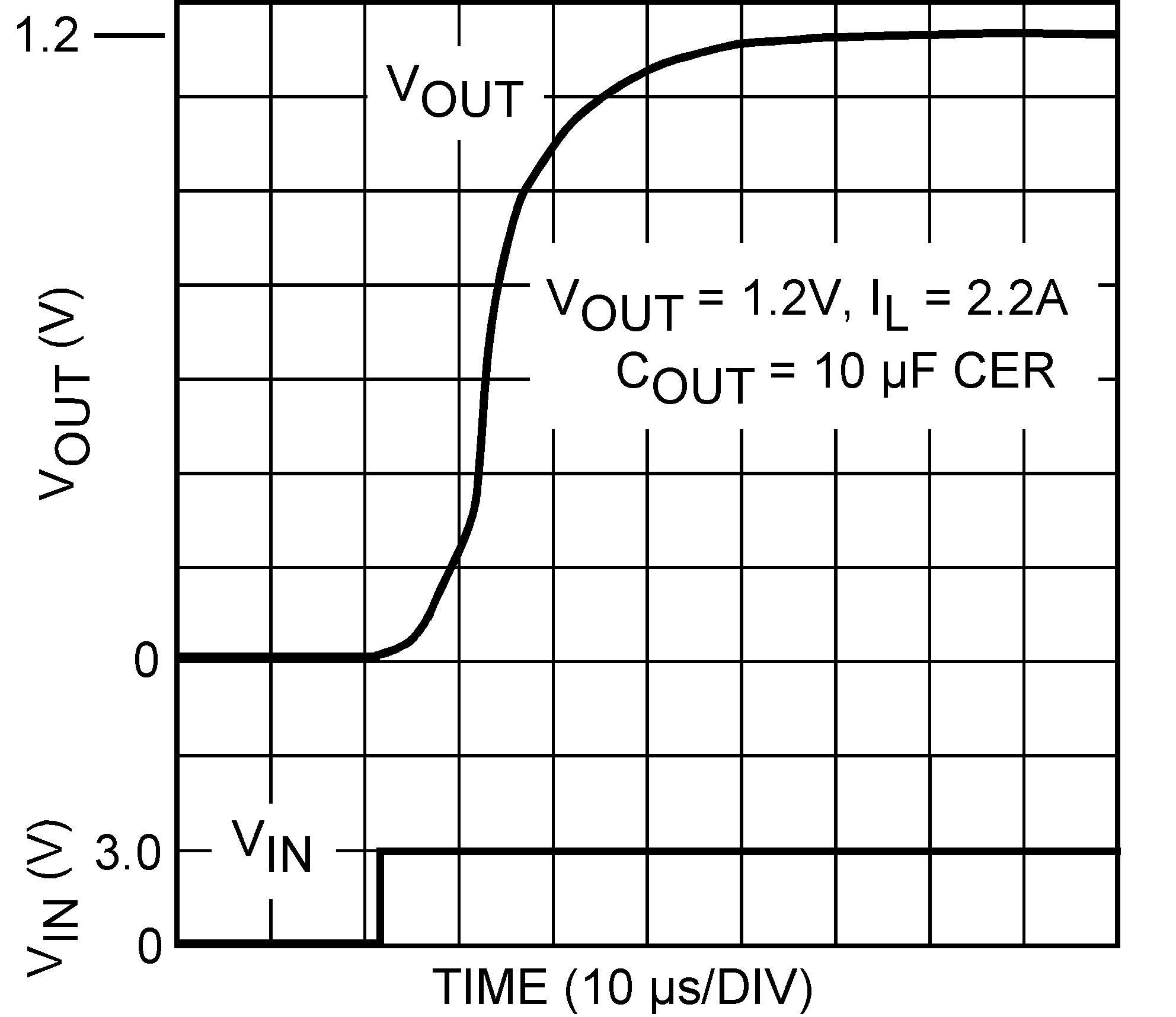
8.2.3 Application Curves

 Figure 28. Load Transient Response: 10-μF Ceramic, 75 A/μs di/dt


