SNVS323I December 2004 – February 2016 LP38690-ADJ , LP38692-ADJ
PRODUCTION DATA.
- 1 Features
- 2 Applications
- 3 Description
- 4 Revision History
- 5 Pin Configuration and Functions
- 6 Specifications
- 7 Detailed Description
-
8 Application and Implementation
- 8.1 Application Information
- 8.2 Typical Application
- 9 Power Supply Recommendations
- 10Layout
- 11Device and Documentation Support
- 12Mechanical, Packaging, and Orderable Information
Package Options
Mechanical Data (Package|Pins)
Thermal pad, mechanical data (Package|Pins)
Orderable Information
7 Detailed Description
7.1 Overview
The LP3869x-ADJ devices are designed to meet the requirements of portable, battery-powered digital systems providing an accurate output voltage with fast start-up. When disabled via a low logic signal at the enable pin (EN), the power consumption is reduced to virtually zero (LP38692-ADJ only). The LP3869x devices perform well with a single 1-μF input capacitor and a single 1-μF ceramic output capacitor.
7.2 Functional Block Diagrams
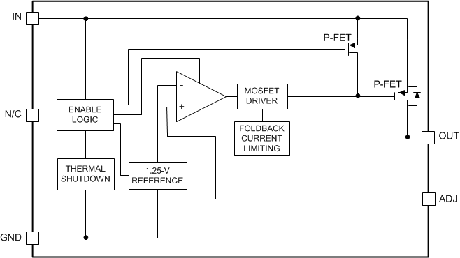
 Figure 27. LP38690-ADJ (WSON)
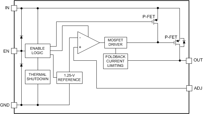
 Figure 28. LP38692-ADJ (SOT-223, WSON)
7.3 Feature Description
7.3.1 Foldback Current Limiting
Foldback current limiting is built into the LP3869x-ADJ which reduces the amount of output current the part can deliver as the output voltage is reduced. The amount of load current is dependent on the differential voltage between VIN and VOUT. Typically, when this differential voltage exceeds 5 V, the load current will limit at about 450 mA. When the VIN –VOUT differential is reduced below 4 V, load current is limited to about 1500 mA.
CAUTION
When toggling the LP38692 EN pin after the input voltage (VIN) is applied, the foldback current limit circuitry is functional the first time that the EN pin is taken high. The foldback current limit circuitry is non-functional the second, and subsequent, times that the EN pin is taken high. Depending on the input and output capacitance values the input inrush current may be higher than expected which can cause the input voltage to droop.
If the EN pin is connected to the IN pin, the foldback current limit circuitry is functional when VIN is applied if VIN starts from less than 0.4 V.
7.4 Device Functional Modes
7.4.1 Enable Pin (LP38692-ADJ Only)
The LP38692–ADJ has an enable pin (EN) which allows an external control signal to turn the regulator output on and off. The enable on/off threshold has no hysteresis. The voltage signal must rise and fall cleanly, and promptly, through the on and off voltage thresholds. The EN pin has no internal pull-up or pull-down to establish a default condition and, as a result, this pin must be terminated either actively or passively. If the EN pin is driven from a source that actively pulls high and low, the drive voltage must not be allowed to go below ground potential or higher than VIN. If the application does not require the enable function, the pin must be connected directly to the IN pin.