SNVS335F December 2006 – November 2016 LP38853
PRODUCTION DATA.
- 1 Features
- 2 Applications
- 3 Description
- 4 Revision History
- 5 Pin Configuration and Functions
- 6 Specifications
- 7 Detailed Description
- 8 Application and Implementation
- 9 Power Supply Recommendations
- 10Layout
- 11Device and Documentation Support
- 12Mechanical, Packaging, and Orderable Information
Package Options
Mechanical Data (Package|Pins)
Thermal pad, mechanical data (Package|Pins)
Orderable Information
1 Features
- Wide VBIAS Supply Operating Range: 3 V to 5.5 V
- Adjustable VOUT Range: 0.8 V to 1.8 V
- Dropout Voltage of 240 mV (Typical) at 3-A Load Current
- Precision VADJ Across All Line and Load Conditions:
- ±1.5% VADJ for TJ = 25°C
- ±2% VADJ for 0°C ≤ TJ ≤ +125°C
- ±3% VADJ for –40°C ≤ TJ ≤ +125°C
- Overtemperature and Overcurrent Protection
- Stable with 10-µF Ceramic Capacitors
- −40°C to +125°C Operating Junction Temperature Range
2 Applications
- ASIC Power Supplies in:
- Desktops, Notebooks, Graphics Cards, and Servers
- Gaming Set-Top Boxes, Printers, and Copiers
- Server Core and I/O Supplies
- DSP and FPGA Power Supplies
- SMPS Post-Regulator
3 Description
The LP38853 is a high-current, fast-response regulator that can maintain output voltage regulation with extremely low input-to-output voltage drop. Fabricated on a CMOS process, the device operates from two input voltages: VBIAS provides voltage to drive the gate of the NMOS power transistor; VIN is the input voltage which supplies power to the load. The use of an external bias rail allows the device to operate from ultra-low VIN voltages. Unlike bipolar regulators, the CMOS architecture consumes extremely low quiescent current at any output load current. The use of an NMOS power transistor results in wide bandwidth, yet minimum external capacitance is required to maintain loop stability.
The fast transient response of this device makes it suitable for use in powering DSP and microcontroller core voltages, and switch-mode power-supply post regulators.
- Dropout Voltage: 240 mV (typical) at 3-A load current
- Low Ground Pin Current: 10 mA (typical) at 3-A load current
- Soft Start: Programmable soft-start time
Device Information(1)
| PART NUMBER | PACKAGE | BODY SIZE (NOM) |
|---|---|---|
| LP38853 | DDPAK/TO-263 (7) | 10.10 mm × 8.89 mm |
| TO-220 (7) | 14.986 × 10.16 mm | |
| SO PowerPAD™ (8) | 4.89 mm × 3.90 mm |
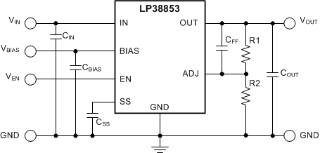
Simplified Schematic
