SNVS335F December 2006 – November 2016 LP38853
PRODUCTION DATA.
- 1 Features
- 2 Applications
- 3 Description
- 4 Revision History
- 5 Pin Configuration and Functions
- 6 Specifications
- 7 Detailed Description
- 8 Application and Implementation
- 9 Power Supply Recommendations
- 10Layout
- 11Device and Documentation Support
- 12Mechanical, Packaging, and Orderable Information
Package Options
Mechanical Data (Package|Pins)
Thermal pad, mechanical data (Package|Pins)
Orderable Information
5 Pin Configuration and Functions
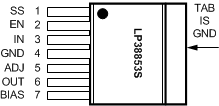
KTW Package
7-Pin DDPAK/TO-263
Top

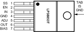
NDZ Package
7-Pin TO-220
Top View

DDA Package
8-Pin SO PowerPAD
Top View

Pin Functions
| PIN | TYPE | DESCRIPTION | |||
|---|---|---|---|---|---|
| NAME | DDPAK/TO-263 | TO-220 | SO PowerPAD-8 | ||
| ADJ | 5 | 5 | 1 | O | The feedback connection to set the output voltage |
| BIAS | 7 | 7 | 3 | I | The supply for the internal control and reference circuitry. |
| EN | 2 | 2 | 6 | I | Device enable, High = On, Low = Off. |
| DAP | — | — | DAP | — | The SO PowerPAD DAP is a thermal connection only that is physically attached to the backside of the die, and used as a thermal heat-sink connection. |
| GND | 4 | 4 | 4 | GND | Ground |
| IN | 3 | 3 | 7 | I | The unregulated voltage input |
| N/C | — | — | 8 | — | No internal connection |
| OUT | 6 | 6 | 2 | O | The regulated output voltage |
| SS | 1 | 1 | 5 | O | Soft-start capacitor connection. Used to control the rise time of VOUT at turnon. |
| TAB | TAB | TAB | — | — | The KTW and NDZ TAB is a thermal and electrical connection that is physically attached to the backside of the die, and used as a thermal heat-sink connection. |