SNVS511U June 2007 – January 2018 LP3907
PRODUCTION DATA.
- 1 Features
- 2 Applications
- 3 Description
- 4 Revision History
- 5 Device Comparison Tables
- 6 Pin Configuration and Functions
-
7 Specifications
- 7.1 Absolute Maximum Ratings
- 7.2 ESD Ratings
- 7.3 Recommended Operating Conditions (Bucks)
- 7.4 Thermal Information
- 7.5 General Electrical Characteristics
- 7.6 Low Dropout Regulators, LDO1 And LDO2
- 7.7 Buck Converters SW1, SW2
- 7.8 I/O Electrical Characteristics
- 7.9 Power-On Reset (POR) Threshold/Function
- 7.10 I2C Interface Timing Requirements
- 7.11 Typical Characteristics — LDO
- 7.12 Typical Characteristics — Bucks
- 7.13 Typical Characteristics — Buck1
- 7.14 Typical Characteristics — Buck2
- 7.15 Typical Characteristics — Bucks
-
8 Detailed Description
- 8.1 Overview
- 8.2 Functional Block Diagram
- 8.3
Feature Description
- 8.3.1 DC-DC Converters
- 8.3.2
SW1, SW2: Synchronous Step-Down Magnetic DC-DC Converters
- 8.3.2.1 Functional Description
- 8.3.2.2 Circuit Operation Description
- 8.3.2.3 PWM Operation
- 8.3.2.4 Internal Synchronous Rectification
- 8.3.2.5 Current Limiting
- 8.3.2.6 PFM Operation
- 8.3.2.7 SW1, SW2 Operation
- 8.3.2.8 SW1, SW2 Control Registers
- 8.3.2.9 Soft Start
- 8.3.2.10 Low Dropout Operation
- 8.3.2.11 Flexible Power Sequencing of Multiple Power Supplies
- 8.3.2.12 Power-Up Sequencing Using the EN_T Function
- 8.3.3 Flexible Power-On Reset (Power Good with Delay)
- 8.3.4 Undervoltage Lockout
- 8.4 Device Functional Modes
- 8.5 Programming
- 8.6
Register Maps
- 8.6.1
LP3907 Control Registers
- 8.6.1.1 Interrupt Status Register (ISRA) 0x02
- 8.6.1.2 Control 1 Register (SCR1) 0x07
- 8.6.1.3 EN_DLY Preset Delay Sequence After EN_T Assertion
- 8.6.1.4 Buck and LDO Output Voltage Enable Register (BKLDOEN) – 0x10
- 8.6.1.5 Buck and LDO Status Register (BKLDOSR) – 0x11
- 8.6.1.6 Buck Voltage Change Control Register 1 (VCCR) – 0x20
- 8.6.1.7 Buck1 Target Voltage 1 Register (B1TV1) – 0x23
- 8.6.1.8 Buck1 Target Voltage 2 Register (B1TV2) – 0x24
- 8.6.1.9 Buck1 Ramp Control Register (B1RC) - 0x25
- 8.6.1.10 Buck2 Target Voltage 1 Register (B2TV1) – 0x29
- 8.6.1.11 Buck2 Target Voltage 2 Register (B2TV2) – 0x2A
- 8.6.1.12 Buck2 Ramp Control Register (B2RC) - 0x2B
- 8.6.1.13 Buck Function Register (BFCR) – 0x38
- 8.6.1.14 LDO1 Control Register (LDO1VCR) – 0x39
- 8.6.1.15 LDO2 Control Register (LDO2VCR) – 0x3A
- 8.6.1
LP3907 Control Registers
- 9 Application and Implementation
- 10Power Supply Recommendations
- 11Layout
- 12Device and Documentation Support
- 13Mechanical, Packaging, and Orderable Information
Package Options
Mechanical Data (Package|Pins)
Thermal pad, mechanical data (Package|Pins)
- RTW|24
Orderable Information
8.3.3 Flexible Power-On Reset (Power Good with Delay)
The LP3907 is equipped with an internal power-on-reset (POR) circuit which monitors the output voltage levels on Bucks 1 and 2. The nPOR is an open drain logic output which is logic LOW when either of the buck outputs are below 91% of the rising value, or when one or both outputs fall below 82% of the desired value. The time delay between output voltage level and nPOR is enabled is (50 µs, 50 ms, 100 ms, 200 ms) 50 ms by default. The system designer can choose the external pullup resistor (that is, 100 kΩ) for the nPOR pin.
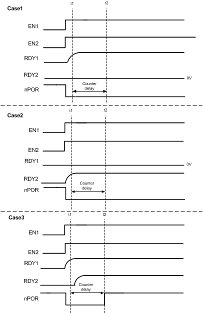
 Figure 35. nPOR with Counter Delay
Figure 35 shows the simplest application of the POR, where both switcher enables are tied together. In Case 1, EN1 causes nPOR to transition LOW and triggers the nPOR delay counter. If the power supply for Buck2 does not come on within that period, nPOR stays LOW, indicating a power fail mode. Case 2 indicates the vice versa scenario if Buck1 supply did not come on. In both cases the nPOR remains LOW.
Case 3 shows a typical application of the POR, where both switcher enables are tied together. Even if RDY1 ramps up slightly faster than RDY2 (or vice versa), then nPOR signal triggers a programmable delay before going HIGH, as explained below.
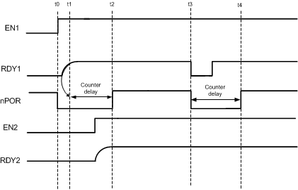
 Figure 36. Faults Occurring in Counter Delay After Start-Up
Figure 36 details the power good with delay with respect to the enable signals EN1, and EN2. The RDY1, RDY2 are internal signals derived from the output of two comparators. Each comparator has been trimmed as follows:
| COMPARATOR LEVEL | BUCK SUPPLY LEVEL |
|---|---|
| HIGH | Greater than 94% |
| LOW | Less than 85% |
The circuits for EN1 and RDY1 is symmetrical to EN2 and RDY2, so each reference to EN1 and RDY1 also works for EN2 and RDY2 and vice versa.
If EN1 and RDY1 signals are High at time t1, then the RDY1 signal rising edge triggers the programmable delay counter (50 μs, 50 ms, 100 ms, 200 ms). This delay forces nPOR LOW between time interval t1 and t2. nPOR is then pulled high after the programmable delay is completed. Now if EN2 and RDY2 are initiated during this interval the nPOR signal ignores this event.
If either RDY1or RDY2 were to go LOW at t3 then the programmable delay is triggered again.
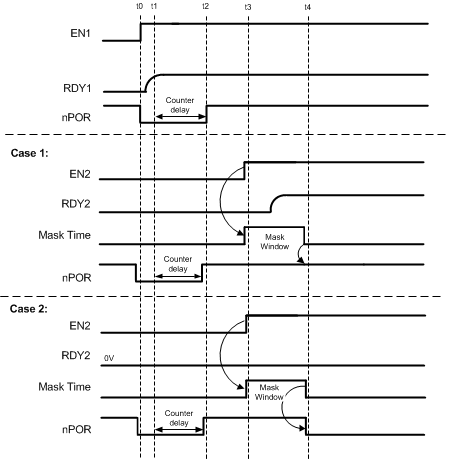
 Figure 37. nPOR Mask Window
If the EN1 and RDY1 are initiated in normal operation, then nPOR is asserted and deasserted as explained in Figure 37.
Case 1 shows the case where EN2 and RDY2 are initiated after triggered programmable delay. To prevent the nPOR being asserted again, a masked window (5 ms) counter delay is triggered off the EN2 rising edge. nPOR is still held HIGH for the duration of the mask, whereupon the nPOR status afterwards depends on the status of both RDY1 and RDY2 lines.
Case 2 shows the case where EN2 is initiated after the RDY1 triggered programmable delay, but RDY2 never goes HIGH (Buck2 never turns on). Normal operation operation of nPOR occurs wilth respect to EN1 and RDY1, and the nPOR signal is held HIGH for the duration of the mask window. We see that nPOR goes LOW after the masking window has timed out because it is now dependent on RDY1 and RDY2, where RDY2 is LOW.
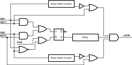
 Figure 38. Design Implementation of the Flexible Power-On Reset
An internal power-on reset of the device is used with EN1, and EN2 to produce a reset signal (LOW) to the delay timer nPOR. EN1 and RDY1 or EN2 and RDY2 are used to generate the set signal (HIGH) to the delay timer. S = R = 1 never occurs. The mask timers are triggered off EN1 and EN2 which are gated with RDY1, and RDY2 to generate outputs to the final AND gate to generate the nPOR.