SNVS481M November 2006 – December 2015 LP3910
PRODUCTION DATA.
- 1 Features
- 2 Applications
- 3 Description
- 4 Revision History
- 5 Device Comparison Tables
- 6 Pin Configuration and Functions
-
7 Specifications
- 7.1 Absolute Maximum Ratings
- 7.2 ESD Ratings
- 7.3 Recommended Operating Conditions
- 7.4 Thermal Information
- 7.5 Electrical Characteristics
- 7.6 Electrical Characteristics: I2C Interface
- 7.7 Electrical Characteristics: Li-Ion Battery Charger
- 7.8 Detection and Timing
- 7.9 Output Electrical Characteristics: CHG, STAT
- 7.10 Output Electrical Characteristics: NRST, IRQB, ONSTAT
- 7.11 Input Electrical Characteristics: USBSUSP, USBISEL
- 7.12 Input Electrical Characteristics: POWERACK, ONOFF, LDO2EN, BUCK1EN
- 7.13 Electrical Characteristics: LDO1 Low Dropout Linear Regulators
- 7.14 Electrical Characteristics: LDO2 Low Dropout Linear Regulator
- 7.15 Electrical Characteristics: Buck1 Converter
- 7.16 Electrical Characteristics: Buck2 Converter
- 7.17 Electrical Characteristics: Buck-Boost
- 7.18 Electrical Characteristics: ADC
- 7.19 I2C Timing Requirements
- 7.20 USB Timing Requirements
- 7.21 Typical Characteristics
-
8 Detailed Description
- 8.1 Overview
- 8.2 Functional Block Diagram
- 8.3
Feature Description
- 8.3.1 Buck1, Buck2: Synchronous Step-Down Magnetic DC-DC Converters
- 8.3.2 Buck-Boost: Synchronous Buck-Boost Magnetic DC-DC Converter
- 8.3.3 Linear Low Dropout Regulators (LDOs)
- 8.3.4 Li-Ion Linear Charger
- 8.3.5 ADC
- 8.3.6 Interrupt Request Output
- 8.3.7 Power-On-Reset
- 8.3.8 Thermal Shutdown and Thermal Alarm
- 8.3.9 NRST Pin
- 8.3.10 Operation Without I2C Interface
- 8.3.11 I2C Master Power Concern
- 8.3.12 System Operation When the Load Current Exceeds the USB or Adapter Current Limit
- 8.3.13 Power Routing
- 8.3.14 Battery Monitor
- 8.3.15 External Power and Battery Detection
- 8.3.16 USB Suspend Mode
- 8.3.17 Setting the USB Current Limit
- 8.3.18 Control Registers
- 8.4 Device Functional Modes
- 8.5 Programming
- 8.6
Register Maps
- 8.6.1 LDO1 Control Register
- 8.6.2 BATTLOW Register (04)H Battery Low Alarm Register
- 8.6.3 PON Register (00)H Power-On Event Register
- 8.6.4 CHCTL Register (01)H Charger Control Register
- 8.6.5 CHSPV Register (02)H Charger Supervisor Register
- 8.6.6 ILIMIT Register (03)H Current Limit Register
- 8.6.7 ADCC Register (0a)H ADC Control Register
- 8.6.8 ADCD Register (0b)H ADC Output Data Register
- 8.6.9 IMR Register (0c)H Interrupt Mask Register
- 8.6.10 IRQ Register (0d)H Interrupt Request Register
- 8.6.11 LDO1 Control Register (08)H
- 8.6.12 LDO2 Control Register
- 8.6.13 Buck1, Buck2 Control Registers and BUCK1EN Pin
- 8.6.14 Buck-Boost Control Register
-
9 Application and Implementation
- 9.1 Application Information
- 9.2
Typical Application
- 9.2.1 Design Requirements
- 9.2.2 Detailed Design Procedure
- 9.2.3 Application Curves
- 10Power Supply Recommendations
- 11Layout
- 12Device and Documentation Support
- 13Mechanical, Packaging, and Orderable Information
Package Options
Mechanical Data (Package|Pins)
- NJV|48
Thermal pad, mechanical data (Package|Pins)
Orderable Information
9 Application and Implementation
NOTE
Information in the following applications sections is not part of the TI component specification, and TI does not warrant its accuracy or completeness. TI’s customers are responsible for determining suitability of components for their purposes. Customers should validate and test their design implementation to confirm system functionality.
9.1 Application Information
The LP3910 is a programmable system power management unit optimized for HDD-based portable media players. The device is intended to connect to an AC-DC wall adapter or USB power source in addition to a lithium-Ion or lithium-polymer single-cell battery. The device can be configured over an I2C interface, or the default configuration stored in EPROM can be used. Additional features such as current and voltage measurements with the ADC or battery thermal monitoring can also be controlled via the I2C interface and interrupt pins.
9.2 Typical Application
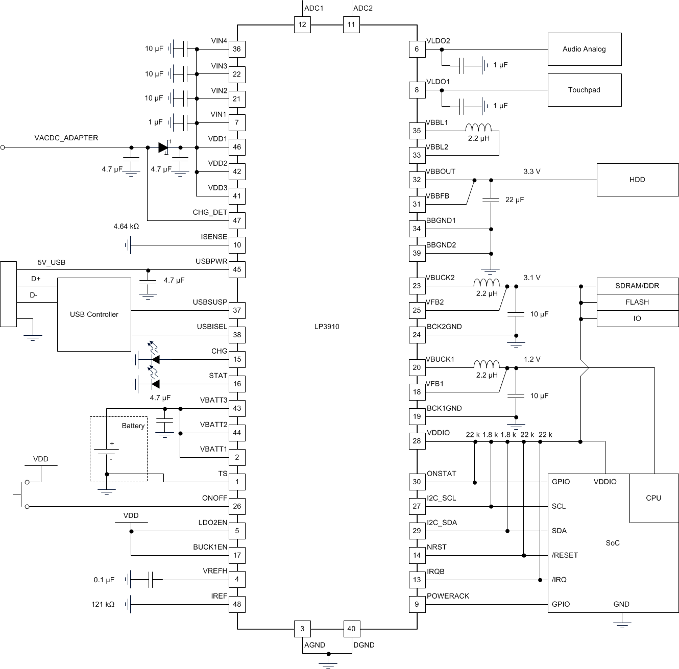 Figure 75. LP3910 Typical Application
9.2.1 Design Requirements
For typical PMU applications, use the parameters listed in Table 15.
Table 15. Design Parameters
| DESIGN PARAMETER | EXAMPLE VALUE |
|---|---|
| Minimum input voltage | 2.7 V |
| Maximum input voltage | 5.5 V |
| LDO1 output voltage | 2.5 V |
| LDO2 output voltage | 3 V |
| Buck1 output voltage | 1.6 V |
| Buck2 output voltage | 1.8 V |
| Buck-Boost output voltage | 3.3 V |
| Charge current | 100 mA |
9.2.2 Detailed Design Procedure
9.2.2.1 Inductors for Buck1, Buck2 and Buck-Boost
There are two main considerations when choosing an inductor; the inductor must not saturate and the inductor current ripple is small enough to achieve the desired output voltage ripple. Care must be taken when reviewing the different saturation current ratings that are specified by different manufacturers.
Saturation current ratings are typically specified at 25°C, so ratings at maximum ambient temperature of the application must be requested from the manufacturer.
There are two methods to choose the inductor saturation current rating:
9.2.2.1.1 Method 1
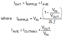
The saturation current is greater than the sum of the maximum load current and the worst-case average-to-peak inductor current. This can be written as Equation 4:

Considered when using the Buck-Boost in boost mode, use Equation 5:
where
- IRIPPLE: Average-to-peak inductor current
- IOUTMAX: Maximum load current
- VIN: Maximum input voltage in application
- L: Minimum inductor value including worst case tolerances (30% drop can be considered for Method 1)
- ƒ: Minimum switching frequency
- VOUT: Output voltage
9.2.2.1.2 Method 2
A more conservative and recommended approach is to choose an inductor that has saturation current rating greater than the maximum current limit.
| INDUCTOR | VALUE | DESCRIPTION | NOTES |
|---|---|---|---|
| LSW1,2 | 2.2 µH | Buck1,2 Inductor | DCR 70 mΩ |
| LBB | 2.2 µH | Buck-Boost Inductor | DCR 70 mΩ |
9.2.2.2 External Capacitors
The regulators on the LP3910 require external capacitors for regulator stability. These are specifically designed for portable applications requiring minimum board space and smallest components. These capacitors must be correctly selected for good performance.
9.2.2.2.1 LDO Capacitor Selection
9.2.2.2.1.1 Input Capacitor
An input capacitor is required for stability. It is recommended that a 1-µF capacitor be connected between the LDO input pin and ground. (This capacitance value may be increased without limit.)
The input capacitor must be located a distance of not more than 1 cm from the input pin and returned to a clean analog ground. Any good-quality ceramic, tantalum, or film capacitor may be used at the input.
NOTE
Tantalum capacitors can suffer catastrophic failures due to surge currents when connected to a low impedance source of power (such as a battery or a very large capacitor). If a tantalum capacitor is used at the input, it should be ensured by the manufacturer to have a surge current rating sufficient for the application.
There are no requirements for the equivalent series resistance (ESR) on the input capacitor, but tolerance and temperature coefficient must be considered when selecting the capacitor to ensure the capacitance remains approximately 1 µF over the entire operating temperature range.
9.2.2.2.1.2 Output Capacitor
The LDOs on the LP3910 are designed specifically to work with very small ceramic output capacitors. A 1-μF ceramic capacitor (temperature types Z5U, Y5V or X7R) with ESR between 5 mΩ to 500 mΩ, are suitable in the application circuit.
Tantalum or film capacitors may also be used at the device output, COUT (or VOUT), but these are not as attractive for reasons of size and cost.
The output capacitor must meet the requirement for the minimum value of capacitance and also have an ESR value that is within the range 5 mΩ to 500 mΩ for stability.
9.2.2.2.1.3 Capacitor Characteristics
The LDOs are designed to work with ceramic capacitors on the output to take advantage of the benefits they offer. For capacitance values in the range of 0.47 µF to 4.7 µF, ceramic capacitors are the smallest, least expensive and have the lowest ESR values, thus making them best for eliminating high frequency noise. The ESR of a typical 1-µF ceramic capacitor is in the range of 20 mΩ to 40 mΩ, which easily meets the ESR requirement for stability for the LDOs.
For both input and output capacitors, careful interpretation of the capacitor specification is required to ensure correct device operation. The capacitor value can change greatly, depending on the operating conditions and capacitor type.
In particular, the output capacitor selection must take account of all the capacitor parameters, to ensure that the specification is met within the application. The capacitance can vary with DC bias conditions as well as temperature and frequency of operation. Capacitor values also show some decrease over time due to aging. The capacitor parameters are also dependent on the particular case size, with smaller sizes giving poorer performance figures in general. As an example, Figure 76 shows a typical graph comparing different capacitor case sizes.
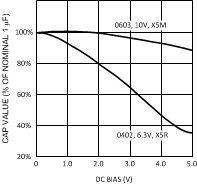 Figure 76. Typical Variation in Capacitance vs DC Bias
As shown in Figure 76, increasing the DC Bias condition can result in the capacitance value that falls below the minimum value given in the recommended capacitor specifications table. Note that Figure 76 shows the capacitance out of spec for the 0402 case size capacitor at higher bias voltages. It is therefore recommended that the capacitor manufacturers’ specifications for the nominal value capacitor are consulted for all conditions, as some capacitor sizes (for example, 0402) may not be suitable in the actual application.
Capacitance of a ceramic capacitor can vary with temperature. The capacitor type X7R, which operates over a temperature range of −55°C to +125°C, only varies the capacitance to within ±15%. The capacitor type X5R has a similar tolerance over a reduced temperature range of −55°C to +85°C. Many large value ceramic capacitors, larger than 1 μF are manufactured with Z5U or Y5V temperature characteristics. Their capacitance can drop by more than 50% as the temperature varies from 25°C to 85°C. Therefore X7R is recommended over Z5U and Y5V in applications where the ambient temperature changes significantly above or below 25°C.
Tantalum capacitors are less desirable than ceramic for use as output capacitors because they are more expensive when comparing equivalent capacitance and voltage ratings in the 0.47-μF to 4.7-μF range.
Another important consideration is that tantalum capacitors have higher ESR values than equivalent size ceramics. This means that while it may be possible to find a tantalum capacitor with an ESR value within the stable range, it would have to be larger in capacitance (which means bigger and more costly) than a ceramic capacitor with the same ESR value. The ESR of a typical tantalum increases about 2:1 as the temperature goes from +25°C down to −40°C, so some guard band must be allowed.
9.2.2.2.1.4 Noise Bypass Capacitors for VREFH Pin
Connecting respectively 100 nF and 1 nF grounded bypass capacitors to the VREFH pin significantly reduces noise on the LDO outputs. VREFH is a high-impedance node connected to a bandgap reference used for the LDOs. Any significant loading on this node causes a change on the regulated output voltages. For this reason, DC leakage current through these pins must be kept as low as possible for best output voltage accuracy. The types of capacitors best suited for the noise bypass capacitors are ceramic and film capacitors. High-quality ceramic capacitors with either NPI or COG dielectric typically have very low leakage. Polypropylene and polycarbonate film capacitors are available in small surface-mount packages and typically have extremely low leakage current. Residual solder flux is another potential source of leakage, which mandates thorough cleaning of the assembled PCBs.
9.2.2.2.2 Buck1, Buck2 and Buck-Boost Capacitor Selection
9.2.2.2.2.1 Input Capacitor Selection for Buck1, Buck2 and Buck-Boost
A ceramic input capacitor of 10 μF, 6.3 V is sufficient for the magnetic DC-DC converters. Place the input capacitor as close as possible to the input of the device. A large value may be used for improved input voltage filtering. The recommended capacitor types are X7R or X5R. Y5V-type capacitors must not be used. DC bias characteristics of ceramic capacitors must be considered when selecting case sizes like 0805 and 0603. The input filter capacitor supplies current to the PFET switch of the DC-DC converter in the first half of each cycle and reduces voltage ripple imposed on the input power source. Low ESR in a ceramic capacitor provides the best noise filtering of the input voltage spikes due to fast current transients. A capacitor with sufficient ripple current rating must be selected. The Input current ripple can be calculated as:

The worse case is when VIN = 2 × VOUT.
9.2.2.2.2.2 Output Capacitor Selection for Buck1, Buck2 and Buck-Boost
A 10-μF, 6.3-V ceramic capacitor must be used on the output of the Buck1 and Buck2 magnetic DC-DC converters. The buck-boost needs a 22-μF capacitor. The output capacitor must be mounted as close as possible to the output of the device. A large value may be used for improved input voltage filtering. The recommended capacitor types are X7R or X5R. Y5V-type capacitors should not be used. DC bias characteristics of ceramic capacitors must be considered when selecting case sizes like 0805 and 0603. DC bias characteristics vary from manufacturer to manufacturer and DC bias curves should be requested from them and analyzed as part of the capacitor selection process.
The output filter capacitor of the magnetic DC-DC converter smooths out current flow from the inductor to the load, helps maintain a steady output voltage during transient load changes and reduces output voltage ripple. These capacitors must be selected with sufficient capacitance and sufficiently low ESD to perform these functions.
The output voltage ripple is caused by the charging and the discharging of the output capacitor and also due to its ESR and can be calculated using Equation 7:

Voltage peak-to-peak ripple due to ESR can be expressed by Equation 8:
Because the VPP-C and VPP-ESR are out of phase, the RMS value can be used to get an approximate value of the peak-to-peak ripple:

The output voltage ripple is dependent on the inductor current ripple and the ESR of the output capacitor (RESR). The RESR is frequency dependent as well as temperature dependent. The RESR must be calculated with the applicable switching frequency and ambient temperature.
Table 16. Recommended Capacitors
| CAPACITOR | MINIMUM VALUE (µF) | DESCRIPTION | RECOMMENDED TYPE |
|---|---|---|---|
| CVDD | 4.7 | Charger input capacitor | Ceramic, 6.3 V, X5R |
| CCHG_DET | 4.7 | Charger input capacitor | Ceramic, 6.3 V, X5R |
| CUSB | 4.7 | USB power (VBUS) capacitor | Ceramic, 6.3 V, X5R |
| CBATT | 4.7 | Li-ion battery capacitor | Ceramic, 6.3 V, X5R |
| CLDO1 | 1 | LDO output capacitor | Ceramic, 6.3 V, X5R |
| CLDO2 | 1 | LDO output capacitor | Ceramic, 6.3 V, X5R |
| CVREFH | 0.1 | Bypass capacitor for internal voltage reference | Ceramic, PolyPropylene and Polycarbonate Film |
| CVIN2,3 | 10 | Buck1, Buck2 input capacitor | Ceramic, 6.3 V, X5R |
| CVBUCK1,2 | 10 | BUCK1,2 output capacitor | Ceramic, 6.3 V, X5R |
| CBB | 22 | Buck-Boost output capacitor | Ceramic, 6.3 V, X5R |
| CVIN1 | 1 | LDO bypass capacitor | Ceramic, 6.3 V, X5R |
| CVIN4 | 10 | Buck and Buck-Boost bypass capacitor | Ceramic, 6.3 V, X5R |
9.2.2.3 Schottky Diode on Charger Input CHG_IN
A Schottky diode is required in the external adapter path to block the reverse current from either the USB or the battery source. The most critical parameter in the selection of the right Schottky diode is the leakage current, which must be below 10 µA over the temperature range in order to prevent false detection of the presence of an external adapter. In addition the Schottky diode must have a maximum voltage rating of 10 V or higher. The current rating depends on the current limit of the adapter. The forward voltage must be limited to 500 mV at its maximum current. The recommended Schottky diode is MBRA210ET3 from ON Semiconductor, which has a reverse leakage current under 1 µA at room temperature and a forward voltage drop of 500 mV at the maximum rated current (IF = 2 A).
9.2.2.4 Resistors
9.2.2.4.1 Battery Thermistor
The LP3910 battery thermistor bias provided by the TS pin is tailored to thermistors with the following specification:
- Negative temperature coefficient
- 100-kΩ resistance
A suitable solution is available from AVX thermistors:
AVXNB21250104 http://www.avxcorp.com/docs/Catalogs/nb21-23.pdf
9.2.2.4.2 I2C Pullup Resistors
I2C_SDA and I2C_SCL pins must have pullup resistors connected to the VDDIO pin. VDDIO must be connected to a power supply that is less than or equal to VDD, such as BUCK2. The values of the pullup resistors (typical approximately 1.8 kΩ) are determined by the capacitance of the bus. A resistor that is too large, combined with a given bus capacitance, results in a rise time that would violate the maximum rise time specification. A resistor that is too small results in a contention with the pulldown transistor on either slave(s) or master.
9.2.2.4.3 RIREF Resistor
The current through this resistor is used as a reference current that biases many analog circuits inside the LP3910 and must have a resistance of 121 kΩ ±1%.
9.2.2.4.4 RISENSE Resistor
The current through this resistor is used as a reference current for the charge current. The accuracy of the ADC is dependent on the tolerance of this resistor. RISENSE must have a resistance of 4.64 kΩ ±1% tolerance.
9.2.3 Application Curves
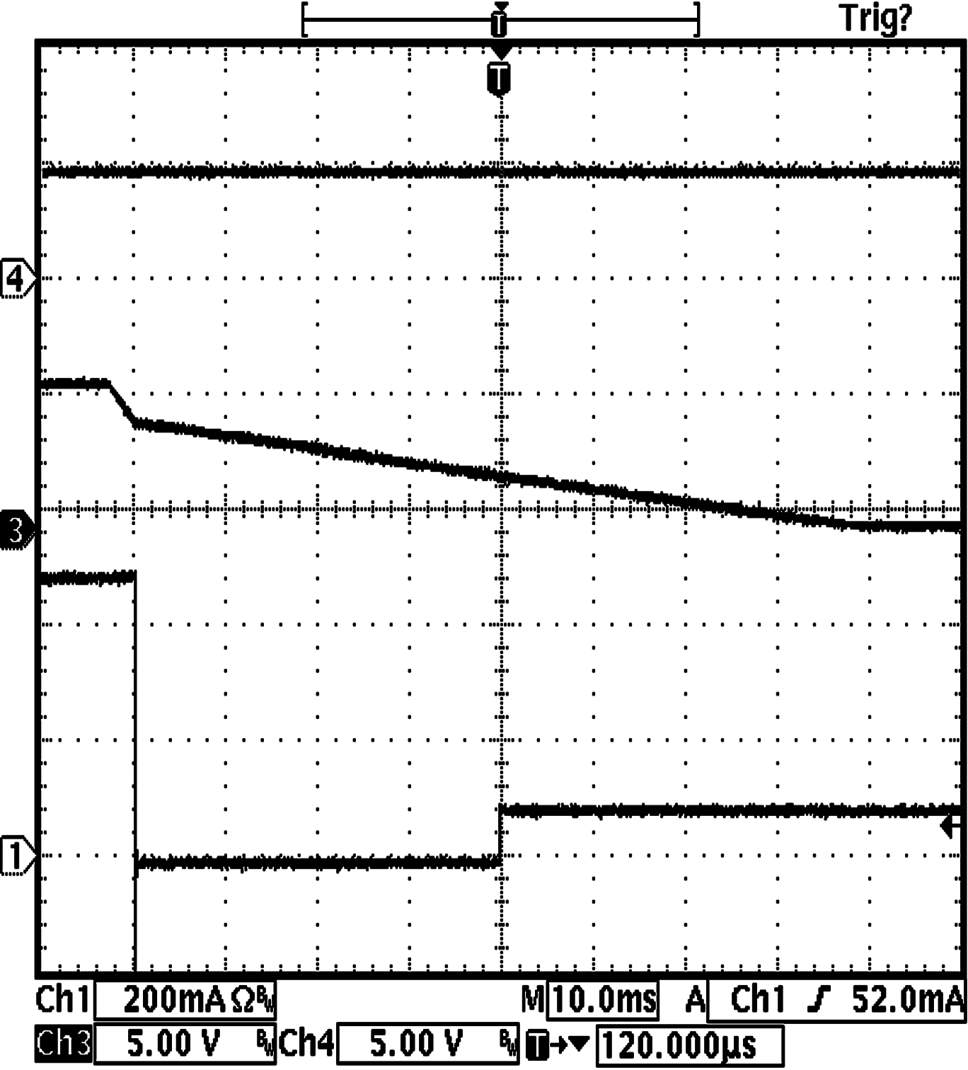
| Ch1 = Charge Current (mA) | Ch4 = USBPWR (V) | |
| Ch3 = CHG_DET (V) | ||
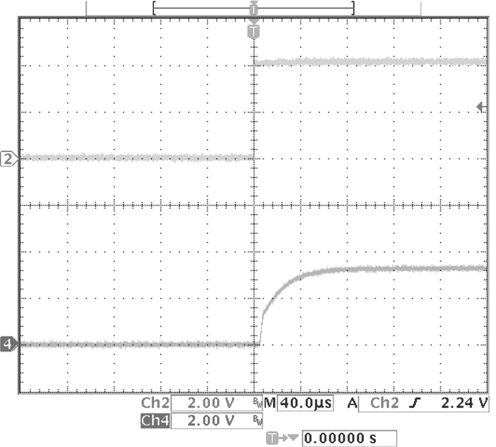
| VIN = 0 to 3.6 V | VOUT = 1.8 V | Load = 1 mA |
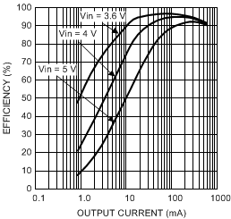
| VOUT = 3.3 V | L = 2.2 µH | Forced PWM Mode |
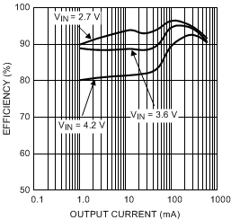
| VOUT = 3.3 V | L = 2.2 μH | PFM-to-PWM Mode |
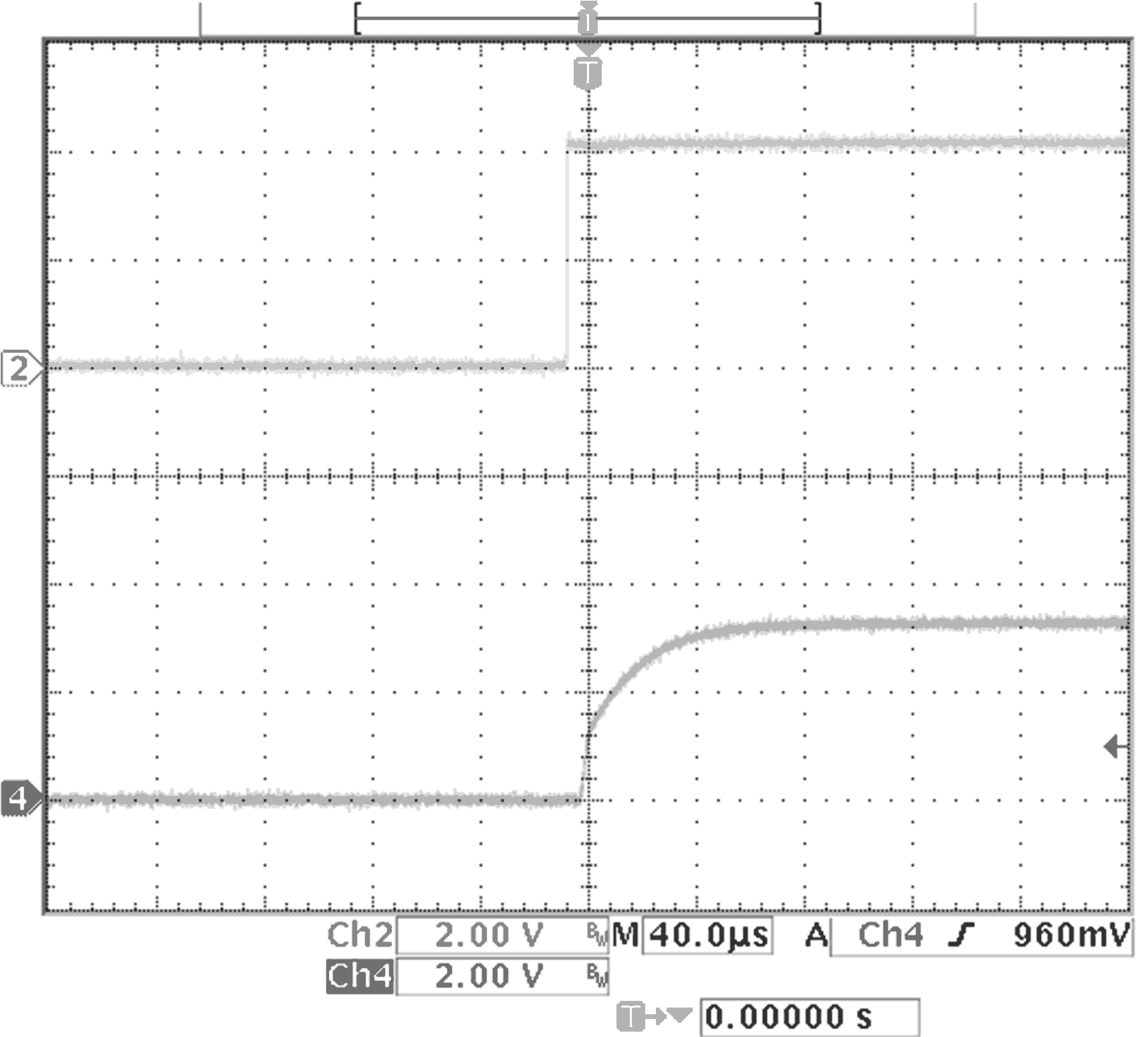
| VIN = 0 to 3.6 V | VOUT = 3.3 V | Load = 1 mA |
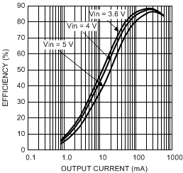
| VOUT = 1.8 V | L = 2.2 µH | Forced PWM Mode |
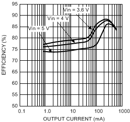
| VOUT = 1.8 V | L = 2.2 µH | PFM-to-PWM Mode |