SNVS481M November 2006 – December 2015 LP3910
PRODUCTION DATA.
- 1 Features
- 2 Applications
- 3 Description
- 4 Revision History
- 5 Device Comparison Tables
- 6 Pin Configuration and Functions
-
7 Specifications
- 7.1 Absolute Maximum Ratings
- 7.2 ESD Ratings
- 7.3 Recommended Operating Conditions
- 7.4 Thermal Information
- 7.5 Electrical Characteristics
- 7.6 Electrical Characteristics: I2C Interface
- 7.7 Electrical Characteristics: Li-Ion Battery Charger
- 7.8 Detection and Timing
- 7.9 Output Electrical Characteristics: CHG, STAT
- 7.10 Output Electrical Characteristics: NRST, IRQB, ONSTAT
- 7.11 Input Electrical Characteristics: USBSUSP, USBISEL
- 7.12 Input Electrical Characteristics: POWERACK, ONOFF, LDO2EN, BUCK1EN
- 7.13 Electrical Characteristics: LDO1 Low Dropout Linear Regulators
- 7.14 Electrical Characteristics: LDO2 Low Dropout Linear Regulator
- 7.15 Electrical Characteristics: Buck1 Converter
- 7.16 Electrical Characteristics: Buck2 Converter
- 7.17 Electrical Characteristics: Buck-Boost
- 7.18 Electrical Characteristics: ADC
- 7.19 I2C Timing Requirements
- 7.20 USB Timing Requirements
- 7.21 Typical Characteristics
-
8 Detailed Description
- 8.1 Overview
- 8.2 Functional Block Diagram
- 8.3
Feature Description
- 8.3.1 Buck1, Buck2: Synchronous Step-Down Magnetic DC-DC Converters
- 8.3.2 Buck-Boost: Synchronous Buck-Boost Magnetic DC-DC Converter
- 8.3.3 Linear Low Dropout Regulators (LDOs)
- 8.3.4 Li-Ion Linear Charger
- 8.3.5 ADC
- 8.3.6 Interrupt Request Output
- 8.3.7 Power-On-Reset
- 8.3.8 Thermal Shutdown and Thermal Alarm
- 8.3.9 NRST Pin
- 8.3.10 Operation Without I2C Interface
- 8.3.11 I2C Master Power Concern
- 8.3.12 System Operation When the Load Current Exceeds the USB or Adapter Current Limit
- 8.3.13 Power Routing
- 8.3.14 Battery Monitor
- 8.3.15 External Power and Battery Detection
- 8.3.16 USB Suspend Mode
- 8.3.17 Setting the USB Current Limit
- 8.3.18 Control Registers
- 8.4 Device Functional Modes
- 8.5 Programming
- 8.6
Register Maps
- 8.6.1 LDO1 Control Register
- 8.6.2 BATTLOW Register (04)H Battery Low Alarm Register
- 8.6.3 PON Register (00)H Power-On Event Register
- 8.6.4 CHCTL Register (01)H Charger Control Register
- 8.6.5 CHSPV Register (02)H Charger Supervisor Register
- 8.6.6 ILIMIT Register (03)H Current Limit Register
- 8.6.7 ADCC Register (0a)H ADC Control Register
- 8.6.8 ADCD Register (0b)H ADC Output Data Register
- 8.6.9 IMR Register (0c)H Interrupt Mask Register
- 8.6.10 IRQ Register (0d)H Interrupt Request Register
- 8.6.11 LDO1 Control Register (08)H
- 8.6.12 LDO2 Control Register
- 8.6.13 Buck1, Buck2 Control Registers and BUCK1EN Pin
- 8.6.14 Buck-Boost Control Register
-
9 Application and Implementation
- 9.1 Application Information
- 9.2
Typical Application
- 9.2.1 Design Requirements
- 9.2.2 Detailed Design Procedure
- 9.2.3 Application Curves
- 10Power Supply Recommendations
- 11Layout
- 12Device and Documentation Support
- 13Mechanical, Packaging, and Orderable Information
Package Options
Mechanical Data (Package|Pins)
- NJV|48
Thermal pad, mechanical data (Package|Pins)
Orderable Information
8 Detailed Description
8.1 Overview
The LP3910 incorporates 2 low-dropout LDO voltage regulators, 2 integrated buck DC-DC converters with dynamic voltage scaling (DVS), one wide load range buck-boost DC-DC converter with programmable output voltage, a 4-channel 8-bit ADC and a dual source Li-ion or Li-polymer battery charger. The charger has the capability to charge and maintain a single cell battery by seamlessly switching between regulated wall adapter and USB power sources. The LP3910 also incorporates advanced battery management functions such as battery temperature measurement, reverse current blocking for USB, LED charger status indication, thermally regulated internal power FETs, battery-voltage monitoring, overcurrent protection, and a 10-hour safety timer.
The buck-boost DC-DC converter targets the power management of hard disk drives and maintains a typical operating voltage of 3.3 V ±5% with a battery voltage below or above this output level. The buck- boost output voltage can be selected to be as low as 1.8 V.
The 4-channel ADC measures the battery voltage and charge current, which can be used for fuel gauging. Two undedicated channels can be used to measure other analog parameters such as discharge current, battery temperature, keyboard resistor scanning and more. The various device parameters are programmable through a 400-kHz I2C-compatible interface.
8.1.1 Two Buck Converters
The LP3910 incorporates two high efficiency synchronous switching buck regulators, Buck1 and Buck2 that deliver a constant voltage from a wall adapter or a single Li-ion battery to the portable system processors, memory and I/O. Using a voltage mode architecture with synchronous rectification, both bucks have the ability to deliver up to 600 mA. Buck1 can output voltages from 0.8 V to 2 V while Buck2 can output voltages from 1.8 V to 3.3 V. Additional features include soft-start, undervoltage lockout, current-overload protection, and thermal-overload protection.
8.1.2 Buck-Boost Converter
The synchronous buck-boost magnetic DC-DC converter supplies power to a hard drive that has a typical 3.3-V operating voltage. This voltage is lower than the maximum battery (4.2 V typically for Li-polymer cells) and higher than the minimum battery (typically 2.8 V). Therefore, in order to provide 3.3 V, regardless of the battery voltage, the buck-boost converter either steps down the battery voltage or steps up the battery voltage. The buck-boost automatically switches between PWM and PFM modes depending on the load and automatically switches between buck and boost modes depending on the battery voltage. The buck-boost converter uses an input voltage from 2.7 V to 5.7 V and generates an output voltage between 1.8 V and 3.3 V for up to 1-A loads.
8.1.3 LDO Regulators
LDO1 is a regulator that can respond to fast transients and is slated for digital loads and high bandwidth analog loads. LDO2 is a linear regulator with a similar architecture but has a slower transient response time with a lower noise performance to supply analog loads. Both regulators can supply up to 150-mA loads and have output voltages that are register programmable through the I2C interface. The LDO1 output voltage is programmable from 1.2 V to 3.3 V, and the LDO2 output voltage is programmable in steps of 100 mV from 1.3 V to 3.3 V.
8.1.4 Battery Charger
The LP3910 can safely charge and maintain a single-cell Li-ion or Li-polymer battery operating off a regulated 6-V automotive adapter, an AC wall adapter, or USB power (VBUS). Input power source selection of USB/adapter is seamless. If present, the charger uses the adapter power regardless of the presence of USB power. The connection of either power source is detected by LP3910. The charger module is a linear charger with constant current pre-qualification, constant current (CC) full-rate charging and constant voltage (CV) charging. CC and CV regulation is performed using an internal power FET Q2 with reverse current blocking. The power FET Q1 acts as a switch with programmable current limit for USB operation.
8.1.5 ADC
The LP3910 is equipped with an 8-bit dual-slope integrating analog-to-digital converter (ADC). Dual-slope converters provide effective filtering of > 500-kHz and < 125-kHz noise components on the input voltage and do not require a sample-and-hold stage. The ADC core digitizes the input voltage ranging from VREF to 2 × VREF, where VREF is the voltage measured on the VREFH pin.
8.1.6 Supply Specification
Table 4 lists the output characteristics of various regulators.
Table 4. Supply Specification
| SUPPLY | LOAD | VOUT (V) | IMAX MAXIMUM OUTPUT CURRENT (mA) | ||
|---|---|---|---|---|---|
| DEFAULT (V) | RANGE (V) | RESOLUTION (mV) | |||
| LDO1 | various | Factory-programmed default | 1.2 to 3.3 | 100 | 150 |
| LDO2 | analog | 1.3 to 3.3 | 100 | 150 | |
| Buck1 | CPU, DSP | 0.8 to 2 | 50 | 600 | |
| Buck2 | I/O, logic, memory | 1.8 to 3.3 | 100 | 600 | |
| Buck-Boost | HD | 1.8 to 3.3 | 50 | 1000 | |
8.2 Functional Block Diagram
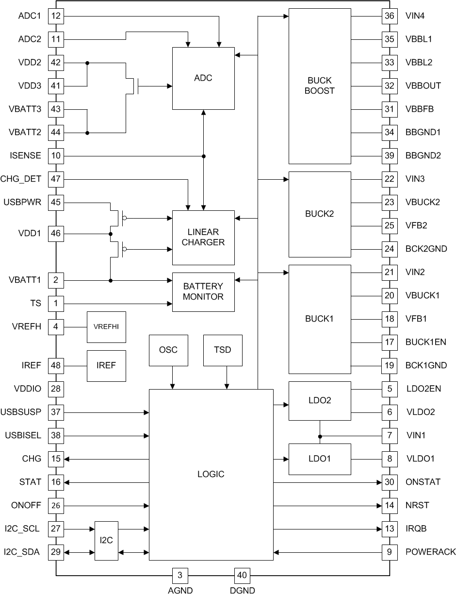
8.3 Feature Description
8.3.1 Buck1, Buck2: Synchronous Step-Down Magnetic DC-DC Converters
The LP3910 incorporates two high-efficiency synchronous switching buck regulators, Buck1 and Buck2, that deliver a constant voltage from a wall adapter or a single Li-ion battery to the portable system processors, memory and I/O. Using a voltage mode architecture with synchronous rectification, both bucks have the ability to deliver up to 600 mA depending on the input voltage and output voltage (voltage headroom), and the inductor chosen (maximum current capability).
There are three modes of operation depending on the current required: PWM, PFM, and shutdown. PWM mode handles current loads of approximately 70 mA or higher, delivering voltage precision of ±3% with 90% efficiency or better. Lighter output current loads cause the device to automatically switch into PFM for reduced current consumption (IQ = 15 µA typical) and a longer battery life. The Standby operating mode turns off the device, offering the lowest current consumption. PWM or PFM mode is selected automatically or PWM mode can be forced through the setting of the buck control register.
Both Buck1 and Buck2 can operate up to a 100% duty cycle (PMOS switch always on). Additional features include soft-start, undervoltage lockout, current overload protection, and thermal overload protection.
8.3.1.1 Buck1, Buck2 Operation
Buck1 is recommended to be used as the processor core supply and has I2C selectable output voltages ranging from 0.8 V to 2 V (typical). Buck2 is recommended for I/O power, Memory power and logic power. Its voltage range can be programmed using the I2C interface from 1.8 V to 3.3 V (typical). The default output voltage for each buck converter is factory programmable (see Application and Implementation).
The system designer can also determine the output voltage of either Buck1 or Buck2 through an external feedback resistor ladder by clearing the output voltage selection field in the Buck1 or Buck2 control registers.
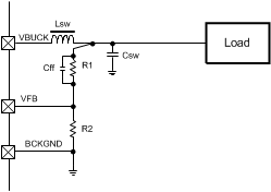 Figure 49. External Control Of Buck Output Voltage Through Feedback Resistor Ladder
8.3.1.2 Circuit Operation Description
A buck converter contains a control block, a switching PFET connected between input and output, a synchronous rectifying NFET connected between the output and ground (BCKGND pin) and a feedback path. During the first portion of each switching cycle, the control block turns on the internal PFET switch. This allows current to flow from the input through the inductor to the output filter capacitor and load. The inductor limits the current to a ramp with a slope of VIN – VOUT / L.
by storing energy in a magnetic field. During the second portion of each cycle, the control block turns the PFET switch off, blocking current flow from the input, and then turns the NFET synchronous rectifier on. The inductor draws current from ground through the NFET to the output filter capacitor and load, which ramps the inductor current down with a slope of –VOUT / L.
The output filter stores charge when the inductor current is high, and releases it when low, smoothing the voltage across the load.
8.3.1.3 PWM Operation
During PWM operation the converter operates as a voltage-mode controller with input voltage feed forward. This allows the converter to achieve excellent load and line regulation. The DC gain of the power stage is proportional to the input voltage. To eliminate this dependence, feed-forward voltage inversely proportional to the input voltage is introduced.
8.3.1.4 Internal Synchronous Rectification
While in PWM mode, the buck uses an internal NFET as a synchronous rectifier to reduce rectifier forward voltage drop and associated power loss. Synchronous rectification provides a significant improvement in efficiency whenever the output voltage is relatively low compared to the voltage drop across an ordinary rectifier diode.
8.3.1.5 Current Limiting
A current limit feature allows the buck to protect itself and external components during overload conditions PWM mode implements cycle-by-cycle current limiting using an internal comparator that trips at 1000 mA (typical).
8.3.1.6 PFM Operation
At very light loads, the converter enters PFM mode and operates with reduced switching frequency and supply current to maintain high efficiency.
The device automatically transitions into PFM mode when either of two conditions occurs for a duration of 32 or more clock cycles:
The inductor current becomes discontinuous or the peak PMOS switch current drops below the IMODE level:

During PFM operation, the converter positions the output voltage slightly higher than the nominal output voltage during PWM operation, allowing additional headroom for voltage drop during a load transient from light to heavy load. The PFM comparators sense the output voltage via the feedback pin and control the switching of the output FETs such that the output voltage ramps between 0.8% and 1.6% (typical) above the nominal PWM output voltage. If the output voltage is below the high PFM comparator threshold, the PMOS power switch is turned on. It remains on until the output voltage exceeds the high PFM threshold or the peak current exceeds the IPFM level set for PFM mode. The typical peak current in PFM mode is:

Once the PMOS power switch is turned off, the NMOS power switch is turned on until the inductor current ramps to zero. When the NMOS zero-current condition is detected, the NMOS power switch is turned off. If the output voltage is below the high PFM comparator threshold (see Figure 50), the PMOS switch is again turned on and the cycle is repeated until the output reaches the desired level. Once the output reaches the ‘high’ PFM threshold, the NMOS switch is turned on briefly to ramp the inductor current to zero and then both output switches are turned off and the part enters an extremely low power mode. Quiescent supply current during this sleep mode is less than 30 µA, which allows the part to achieve high efficiencies under extremely light load conditions. When the output drops below the low PFM threshold, the cycle repeats to restore the output voltage to approximately 1.6% above the nominal PWM output voltage.
If the load current increases during PFM mode (see Figure 50) causing the output voltage to fall below the ‘low2’ PFM threshold, the device automatically transitions into fixed-frequency PWM mode.
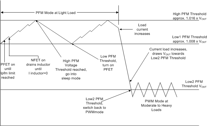 Figure 50. Operation in PFM Mode and Transfer to PWM Mode
8.3.2 Buck-Boost: Synchronous Buck-Boost Magnetic DC-DC Converter
The LP3910 is equipped with a synchronous buck-boost magnetic DC-DC converter to supply power to the hard drive that has a typical 3.3-V operating voltage. This voltage is lower than the maximum battery (4.2 V typically for Li-polymer cells) and higher than the minimum battery (typically 2.8 V). Therefore, in order to provide 3.3 V, regardless of the battery voltage, the Buck-Boost converter either steps down the battery voltage or steps up the battery voltage. The Buck-Boost automatically switches between PWM and PFM modes depending on the load and automatically switches between buck and boost modes, depending on the battery voltage.
By setting bit D6 of the Buck-Boost control register, the Buck-Boost is forced to operate using PWM modulation regardless of the load. By default this bit is cleared.
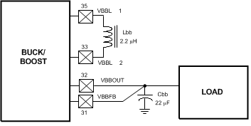 Figure 51. Schematic Section for Buck-Boost Operation
8.3.3 Linear Low Dropout Regulators (LDOs)
LDO1 is a regulator that can respond to fast transients and is slated for digital loads and high bandwidth analog loads. LDO2 is a linear regulator with a similar architecture but has a slower transient response time with a lower noise performance to supply analog loads. The output voltages of both LDOs are register programmable through the I2C interface. The default output voltages are factory programmed during final test.
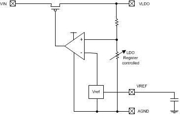 Figure 52. LDO Architecture Diagram
8.3.3.1 No-Load Stability
The LDOs remain stable and in regulation with no external load. This is an important consideration in some circuits, for example, CMOS RAM keep-alive applications.
8.3.4 Li-Ion Linear Charger
8.3.4.1 Charger Architecture
The LP3910 can safely charge and maintain a single cell Li-ion or Li-polymer battery operating from a regulated 6-V car adapter, AC wall adapter, or USB power (VBUS). Input power source selection of USB/adapter is seamless. If present, the charger uses the adapter power regardless of the presence of USB power. The connection of either power source is detected by the LP3910 device.
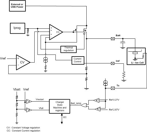 Figure 53. Charger Architecture
The charger module is a linear charger with constant current pre-qualification, CC full-rate charging and CV charging. CC and CV regulation is performed using an internal Power FET Q2 with reverse current blocking. The termination voltage is controlled to within ±0.35% at room temperature.
The power FET Q1 acts as a switch with programmable current limit for USB operation.
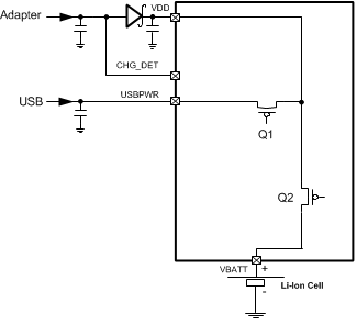 Figure 54. Switches for USB Charging Path
8.3.4.2 Charge Status Indication
Two LEDs connected to the LP3910 are used to indicate the status of the charging. The CHG pin is connected to a red LED that is enabled when an external power source is connected and the battery is charging. The second STAT pin is connected to a green LED. When the battery charging transitions from CC to CV mode, then the green LED is blinking with a 50% duty cycle and a period of 1 second. When the battery is fully charged, then the green LED is always on.
Both LEDs are off when there is no external power connected.
Table 5. Truth Table for the LED Status Indicators
| CONDITION | RED LED | GREEN LED |
|---|---|---|
| No Charger or USB | OFF | OFF |
| Charger off | ON | OFF |
| Pre-Qualification | ON | OFF |
| Constant Current CC | ON | OFF |
| Constant Voltage CV | ON | 50% duty cycle |
| EOC / Top-OFF charging | ON | ON |
| Charge cycle complete | ON | ON |
| ERROR (Battery Temperature, Thermal shutdown) | 50% duty cycle | OFF |
| Safety Timer Expired | 50% duty cycle | OFF |
50% duty cycle indicates the LED is pulsed on and off for equal times at a frequency of 1 Hz.
The RED pin and GREEN pin are connected to a regulated driver to ensure that the brightness is independent from the external power. The LEDs need to be connected between the CHG and STAT pins and GND.
8.3.4.3 Thermal Charger Power FET Regulation
The internal power FET Q2 in the linear charger module is thermally regulated to the junction temperature of 115°C to ensure optimal charging of the battery. The charge current is limited by the charge current selected in the charger control register but is also thermally limited to prevent the junction from overheating during high charge currents at high ambient temperatures as the package power dissipation is limited.
Thermal regulation ensures maximum charge current and superior charge rate without exceeding the power dissipation limits of LP3910 device.
8.3.4.4 Battery Charger Operating Modes
8.3.4.4.1 Pre-Qualification Mode
Lithium batteries cannot be subjected to a high current when the battery voltage is under a certain threshold, otherwise the longevity of the battery would be compromised. Below this threshold of VFULLRATE, which typically measures 2.85 V, the charger circuit supplies a pre-qualification charge current. If the wall adapter is charging the battery, the charger circuit supplies a constant current of 10% of the programmed charge current. If the USB is charging the battery, the charger circuit supplies a constant 50-mA charge current. When the battery voltage reaches VFULL_RATE, the charger transitions from pre-qualification to full-rate charging. In pre-qualification mode, the STAT2, STAT1, and STAT0 bits in the charger supervisory register are respectively low, low, high.
8.3.4.4.2 Full-Rate Charging Mode
The full-rate charge cycle is initiated following the successful completion of the pre-qualification mode. During full-rate charging, the battery voltage steadily increases while charged with a CC. The three charger status bits STAT2, STAT1, and STAT0 are respectively low, high, and low. The full-rate charge current is selected using the charge control register, which defaults to 100 mA.
Charging Li-ion batteries at a rate of 1C is recommended (where C is the capacity of the battery). As an example, it is recommended to charge a battery with a capacity of 800 mA at 800 mA, or 1C. Charging at a higher rate may compromise the quality and lifetime of the battery.
8.3.4.4.3 Constant-Voltage (CV) Charging Mode
The battery voltage increases rapidly as a result of full-rate charging and once it reaches the programmable termination voltage of either 4.1 V, 4.2 V or 4.38 V, the charger moves to constant-voltage charge mode. During this mode, the charge current gradually decreases while the battery remains at the termination voltage. The termination voltage can be selected to be either 4.1 V, 4.2 V or 4.38 V by programming bits D6 and D7 in the Charger Control register to accommodate different battery chemistries. In CV charging mode, the Charge Control Status bits STAT2, STAT1 and STAT0 are respectively logic 0, logic 1, and logic 1.
8.3.4.4.4 Top-Off Charging Mode
When the charge current reduces to the EOC threshold (programmable to 5% or 10% of programmed full rate charge current), constant voltage charging continues for an additional 21 minute TOP-OFF time period. In TOP-OFF charging mode, the Charge Control Status bits STAT2, STAT1 and STAT0 are respectively logic 1, logic 1 and logic 1. At the end of the TOP-OFF period, the charger transitions to Charge Cycle Complete.
8.3.4.4.5 Charge Cycle Complete
During charge cycle complete, the charger is automatically disabled, regardless of the state of the charge enable bit. In charge cycle complete, the STAT2, STAT1 and STAT0 bits are respectively logic 1, logic 0, and logic 1. When the battery voltage drops below the VRESTART threshold, charging resumes in full-rate charging mode.
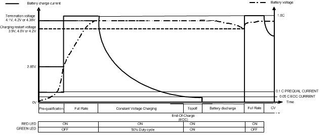 Figure 55. Charge Cycle Complete
8.3.4.5 Battery Temperature Monitoring (TS Pin)
The LP3910 is equipped with a battery thermistor terminal to continuously monitor the battery temperature by measuring the voltage between the TS pin and GND. With the TS pin connected to the battery thermistor, charging is allowed only if the battery temperature is within the acceptable temperature range set by a pair of internal comparators inside the LP3910. The temperature window is 0°C to 45°C or 0°C to 50°C, depending on the setting of D2 of the charger supervisory (CHSPV) register. There is 3°C of temperature hysteresis associated with each temperature threshold. The default temperature range is 0°C to 50°C and can be changed to 0°C to 45°C by setting bit D3 in the CHSPV register. If the battery temperature is out of range, STAT2, STAT1, and STAT0 bits in the CHSPV register are set to logic1, logic0, logic0, and charging is suspended.
The TS pin is only active during charging and draws no current from the battery when no external power source is present.
If the TS pin is not used in the application, it must be connected to GND through a 100-kΩ pulldown resistor.
When the TS pin is left floating (battery removal), the charger is disabled as the TS voltage exceeds the lower temperature limit.
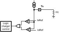 Figure 56. Battery Temperature Monitor with TS Pin
8.3.4.6 Disabling Charger
Charging can be safely interrupted by clearing the Charge enable bit D1 in the Charge Control Register and can subsequently resume upon setting this bit. When the charger is disabled, STAT2, STAT1, and STAT0 bits in the CHSPV register are set to logic 0.
8.3.4.7 Safety Timer
In order to prevent endless charging, which could degrade the battery quality and life time, the LP3910 contains a safety timer that limits charging regardless whether the battery has reached its full capacity or not. In prequalification the safety timer is 1 hour. In full rate or constant voltage charging the safety timer is a maximum of 10 hours minus the time in prequalification.
When the timer times out of uninterrupted charging, an IRQ is generated to alert system processor. The status of the timer can also be polled by reading the IRQ register if the system doesn’t support hardware interrupts.
The safety timer resets and starts counting from zero upon the following events:
- Power ON (through connecting valid power to either USBPWR or CHGN_IN pins).
- Interchanging USBPWR and CHG_IN sources.
- The voltage of a charged battery drops below the restart value, and the charger is enabled.
- Disabling and re-enabling of the charger by toggling bit D1 of the Charge Control Register.
- Emerging from thermal shutdown.
- Emerging from a battery temperature out-of-range, and the charger is enabled.
- Emerging from USB suspend mode when charging with USB power.
8.3.4.8 Charging Maintenance
When a fully charged battery is being loaded by the system while the external power is present and while bit D1 in the charge control register is set to a 1 (charge enable) then the charging restarts when the battery voltage drops below the charging restart threshold. The value of the threshold depends on the termination voltage according to the following table:
Table 6. Charging Thresholds
| VTERM | CHARGING RESTART VOLTAGE |
|---|---|
| 4.1 V | 3.9 V |
| 4.2 V | 4 V |
| 4.38 V | 4.2 V |
8.3.5 ADC
The LP3910 is equipped with an 8-bit dual-slope integrating an ADC. Dual-slope converters provide effective filtering of > 500-kHz and < 125-kHz noise components on the input voltage, and does not require a sample and hold stage. The ADC core digitizes the input voltage ranging from VREF to 2VREF, where VREF is the voltage measured on the VREFH pin. After an initial 2-ms warm-up for the first activation of the ADC enable bit, the dual-slope converter integrates the input signal during the first phase for approximately 2 ms, followed by a second phase that integrates VREF for 0 ms to 2 ms depending on the level of the input signal. As a result the total conversion time varies from 2 ms to 4 ms.
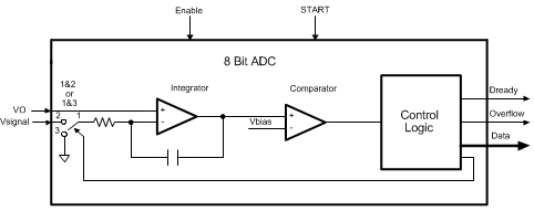 Figure 57. Simplified ADC Block Diagram
The ADC multiplexes 4 different sources:
- The battery voltage
- The battery charge current
- External source ADC1
- External source ADC2
The voltage ranges for the first two sources are scaled to match the input voltage interval of the ADC: [VREFH, 2VREFH]. This is accomplished by using two internal scalars.
8.3.5.1 Battery Voltage Measurement
The battery voltage scalar transforms the battery voltage ranging from 2.6 V to 3.5 V to the reference voltage interval: [VREFH, 2*VREFH]. A wider voltage range (2.6 V to 4.4 V) can be selected through I2C by setting the voltage range bit D7 in register 0xA to 0’b1.
8.3.5.2 Battery Charge Current Measurement
The battery charge current is indirectly measured by measuring the voltage across the ISENSE resistor, RSENSE. A fixed portion of the battery charge current is mirrored over the RSENSE as in Equation 3:
where K is a ratio between the ISENSE current and the charge current.
The battery charge current scalar transforms the voltage across the external ISENSE resistor to the [VREFH, 2 × VREFH] input voltage interval of the ADC.
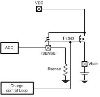 Figure 58. Battery Charge Scalar
8.3.5.3 External General-Purpose Sources
Two additional ADC sources are available on the ADC1 and ADC2 pins of the LP3910. These two external ADC sources are not internally scaled and have an input voltage range of [VREFH, 2 × VREFH]. The system designer can use these two sources for general-purpose applications such as resistive keyboard matrix scanning, temperature measurements, battery load current, battery ID resistor measurement, and others.
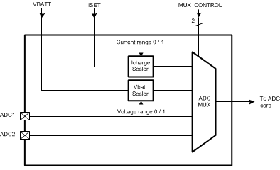 Figure 59. ADC Analog Front-End Block Diagram
The source selection and the access to the conversion results are established through the I2C linked control registers: ADCC and ADCD.
The ADC is by default disabled to minimize current consumption and must be enabled by setting D2 in the ADCC register. Writing a logic 1 to bit D3 in the ADC initiates a conversion. It is advised to select the correct ADC source before a conversion is started. The ADC sets bit D4 in the ADCC register upon the completion of a conversion, which is typically 4 ms after the start of the conversion. At the same time an interrupt request is generated. (See IRQ Register (0d)H Interrupt Request Register).
To save power, disable the ADC by setting bit 2 of D2 to 0. To make repetitive starts, set bit D3 to 0 then to 1 for register 0Ah to initiate start of conversion. The interrupt driven protocol between LP3910 and the system processor is the most efficient way to acquire data from successive measurements as shown in Figure 60:
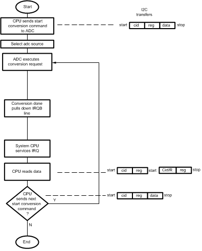 Figure 60. Data Measurement and Acquisition Sequence
8.3.6 Interrupt Request Output
The LP3910 has the ability to interrupt the system processor through the open drain IRQB pin, which transitions to an active logic low level upon the following 8 events:
- USB Power detected
- USB disconnected
- CHG_IN Power detected
- CHG_IN disconnected
- Battery low alarm
- Thermal alarm
- ADC conversion completed
- Charger safety timer time-out
The events form the interrupt sources that correspond to a certain bit location in the interrupt request (IRQ) register. All interrupt sources can be masked by the interrupt mask register (IMR). Masking the interrupt prevents the interrupt event from asserting the IRQB pin, yet the event is still captured in the IRQ register, which allows the processor to poll the interrupt sources.
After an active low IRQB has been detected by the system processor, the latter services the interrupt and accesses the IRQ register to determine which source was responsible for the interrupt request. Reading the IRQ register automatically clears the register to enable the capture of the next interrupt events.
As new interrupts can occur while the I2C read cycle is clearing the IRQ register, a buffer register called interrupt pending register (IPR), not accessible through the I2C-compatible interface holds the next interrupts. De-asserting the IRQB output is immediately followed by a new transition of IRQB to logic low when an interrupt is pending.
The Interrupts are not hardware prioritized. It is up to the firmware to determine the priority in case more than one interrupt request is set.
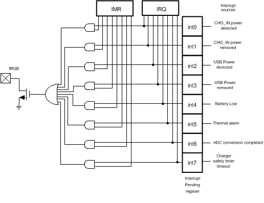 Figure 61. Interrupt Request Setting
8.3.6.1 Interrupts and Standby Mode
Interrupts are captured in standby mode and can be serviced when the system processor is enabled when the LP3910 is in an active state.
8.3.6.2 Interrupt Sources
- CHG_IN Power Detected and CHG_IN Disconnect (INT0 and INT1): An interrupt (INT0) is generated when CHG_IN power is connected to the LP3910. Another interrupt (INT1) is generated upon CHG_IN power removal.
- USB Power Detected and USB Disconnect (INT2 and INT3): An interrupt (INT2) is generated when USB power is connected to the LP3910. Another interrupt (INT3) is generated upon disconnecting the USB power.
- Battery Low (INT4): When the battery voltage drops below the battery low threshold IRQ, an interrupt is generated. This allows the processor to perform some routine tasks prior to going to standby mode.
- Thermal Alarm (INT5): If the junction temperature of the LP3910 exceeds 115°C, an interrupt is generated.
- ADC Conversion Done (INT6): The ADC generates an interrupt request upon the completion of a data conversion.
- Charger Timer Interrupt (INT7): A charger timeout occurs 10 hours after it started (see Li-Ion Linear Charger) and subsequently requests an interrupt.
8.3.7 Power-On-Reset
The LP3910 is equipped with an internal power-on-reset (POR ) circuit that resets the logic when VDD < VPOR. This ensures that the logic is properly initialized when VDD rises above the minimum operating voltage of the logic and the internal oscillator that clocks the sequential logic in the control section.
8.3.8 Thermal Shutdown and Thermal Alarm
An internal temperature sensor monitors the junction temperature of the LP3910. This sensor forcibly invokes standby mode in the unusual case of the junction temperature of the silicon exceeding the normal operating level due to excessive loads on all power regulators, the Li-ion charger, or due to an abnormally high ambient temperature. The thermal shutdown threshold is 160°C.
The thermal shutdown is preceded by a thermal alarm that generates an interrupt request if unmasked. The temperature threshold for triggering the alarm is 115°C.
8.3.9 NRST Pin
The NRST pin is an open-drain output and is active low during standby, power-off and charger standby modes. The NRST timing is determined by a factory programmable counter.
8.3.10 Operation Without I2C Interface
Operation of the LP3910 without the I2C interface is possible if the system can operate with default values for the DC-DC converters and the charge (see Table 3). The I2C-less system must use the POWERACK pin to power cycle the LP3910.
8.3.11 I2C Master Power Concern
The processor that contains the I2C master must be powered by BUCK1 or LDO2 as these converters require no I2C access to enable/disable them. If the I2C master were to be powered by a DC-DC converter that is enable/disabled through a control register, then a corrupted application software execution could by accident disable the power to the I2C master, which in this case has no means to recover. It is possible that the regulator connected to VDDIO may accidentally disable, in which case the processor should recognize that communication has been broken, then power down the system to allow for a clean restart.
8.3.12 System Operation When the Load Current Exceeds the USB or Adapter Current Limit
In the event that the system requires current that exceeds the current limit of either the USB or the adapter source, then the battery can provide the extra power provided that it has been charged. It is clear that a long sustained overload eventually discharges the battery such that its extra power is no longer be sufficient to properly operate the system. This is the case when the system is for instance operated from a USB host with a 100-mA current limit.
8.3.13 Power Routing
The LP3910 power can originate from three different sources: Adapter power, USB power, or battery power. The objective of the power routing is to be able to:
- Operate the portable system from external power regardless of the battery voltage.
- Operate the portable system from USBPWR when the battery exceeds the full-rate qualification threshold voltage (VFULLRATE).
- Concurrently charging and operating the system when external power is present
- Seamless selection of Adapter or USB power as the primary external power source
Power Routing supports 4 modes:
- A regulated external adapter power is present and concurrently supplies the system power and the battery charger.
- USB power is present and supplies the system and the battery.
- USB power is present but the system demand exceeds the USB current limit, so that the battery provides the additional power to operate the system.
- The battery is the sole supply source to the system when no external power source is present
The current flows in the different modes are realized through internal FETS and an external Schottky as shown in Figure 62:
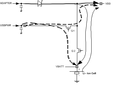 Figure 62. Charging and Sourcing Current Paths
The current provided by the external adapter power or USB power, when inserted, first supplies the system load; the remainder is used for charging.
The different paths are configured through two internal power FETs, Q1 and Q2, and an external Schottky diode. Q1 is a power FET that is only active during USB charging. Q2 functions either as a linear power FET during charging or as a low RDSON switch when no external power is present, and the battery discharges to supply power to the system.
Table 7. Power Routing Options
| POWER ROUTE | Q1 | Q2 |
|---|---|---|
| Regulated adapter supply & battery charging | OFF | Regulated |
| USB supply & battery charging | ON | Regulated |
| No external supply and battery discharging | OFF | ON |
The power routing function allocates power to the system through the VDD pin and to the battery. VDD1, VDD2, VDD3, VIN1, VIN2, VIN3, and VIN4 must be connected together externally. VBATT1, VBATT2, and VBATT3 must be connected together externally.
8.3.14 Battery Monitor
The battery voltage is monitored and invokes the power-off mode when the battery low threshold is breached for more than 5 ms (typical). The battery-low threshold DEFAULT is factory programmed. The battery low threshold range is 2.5 V to 3.5 V with steps of 50 mV. The battery-low threshold in the table below refers to a decreasing battery voltage. The threshold when the battery voltage is transitioning out of the VBATTLOW is 50 mV (typical) higher than the values listed in the table below due to a built-in hysteresis of 50 mV (typical).
The battery low IRQ is triggered 200 mV above the battery low alarm threshold that powers down the device. This gives the user time for a controlled shutdown.
8.3.15 External Power and Battery Detection
When a wall adapter is detected, regardless of the battery voltage, the LP3910 moves to the active mode and the power-up sequencer is started. Similar to the ONOFF pin, there is a 32-ms deglitch time to ensure a clean wall adapter detection and the system processor must set the PACK bit (D4) in the PON register or the POWERACK pin within 128 ms (maximum) of the start of the power-up sequencer.
When USB PWR is detected, and the battery is above the low-battery-alarm threshold, the LP3910 moves to the active mode, and the power-up sequencer is started. As with the ONOFF pin, there is a 32-ms deglitch time to ensure a clean USB detection, and the system processor must set the PACK bit (D4) in the PON register or the POWERACK pin within 128 ms (maximum) of the start of the power-up sequencer. If the battery is below the low-battery-alarm threshold, the system remains powered down until the USBPWR charges the battery up to the low-battery-alarm threshold, at which point the power-up sequencer is started.
The four LSB bits of the PON register indicate which PON source moves the LP3910 device out of standby and into active mode:
- Battery insert
- ONOFF push button
- CHG_IN detect (connection of power adapter)
- USB power (plug-in of powered USB cable)
These bits are cleared upon powering off.
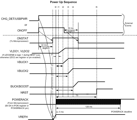 Figure 63. Power-Up Sequence
8.3.16 USB Suspend Mode
The LP3910 USB current consumption can be disabled during suspend mode through a dedicated pin (USBSUSP). Applying a logic 1 to this pin disables the USB current path, and current is reduced to input leakage current less than 30 µA on the USBPWR pin.
8.3.17 Setting the USB Current Limit
The USB current that is available from the USB on the VBUS wire is limited by default to 100 mA. More current (up to 800 mA) can be negotiated through a session request protocol between host and peripheral. The USB current limit must be signaled to the LP3910 by means of the USBISEL pin or the ILIMIT register as indicated below:
- If the USB current limit is 100 mA then the USB controller of the peripheral system must set the USBISEL logic 0 or by setting the ILIMIT register bits [D1, D0] to 2’b00.
- If the USB current limit is 500 mA, the USB controller must apply logic 1 to the USBISEL pin or change the ILIMIT register accordingly. Under this condition, the LP3910 allows charging with a charge current that is determined by the charge control register, not exceeding 500 mA.
The LP3910 prevents (through internal circuitry) the charge current from exceeding the USB current limit, even if the current setting in the Charge Control Register exceeds 500 mA.
The controller can also select a USB current limit of 800 mA through I2C that exceeds current USB spec values.
8.3.18 Control Registers
The LP3910 contains 14 user-programmable registers that configure the functionality of the individual modules inside the device. Registers are programmed through an I2C interface and have default values that are invoked during an internal reset. Some of the default values can be tailored to the specific needs of the system designer.
8.4 Device Functional Modes
The LP3910 can be in 3 different operating modes as shown in Figure 64:
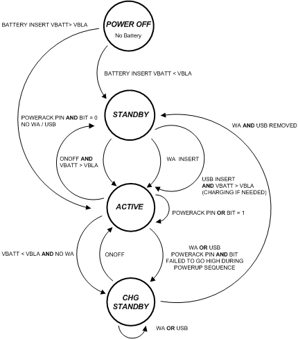 Figure 64. Operating Mode State Diagram
8.4.1 State Machine Definitions
-
VBLA Battery low alarm threshold
-
VBATT Battery voltage
-
WA Wall Adapter
-
USB Universal Serial Bus Adapter
-
ONOFF On off pin event
-
POWERACK Acknowledgment from the Host Processor
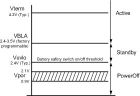 Figure 65. Voltage Threshold Levels
Table 8. Power State Table
| POWER OFF | STANDBY | ACTIVE | CHARGER STANDBY | |
|---|---|---|---|---|
| LDO1,2 | Off | Off | On | Off |
| Buck1,2 | Off | Off | On | Off |
| Buck-Boost | Off | Off | On | Off |
| Charger | Off | Off | On if Charger / USB Present | On if Charger / USB Present |
| ADC | Off | Off | On | Off |
| NRST | Low | Low | High | Low |
| I2C interface | Off | Off | On | On |
| Internal system oscillator | Off | Off | On | On |
| Battery monitor | Off | On | On | On |
| Current consumption | <1 µA | 10 µA (typical) | See Specifications | See Specifications |
8.4.1.1 Power-Off Mode
In power-off mode the main battery, the battery charger supply, and the USB supply are below their minimum on levels. All internal circuits are disabled as the supply voltage is below the level to activate them. The LP3910 is in power-off mode when the battery voltage is below the battery VUVLO (2.4 V, typical) except when a valid external supply is detected.
8.4.1.2 Standby Mode
When the LP3910 is in standby mode, the chip is waiting for a valid power-on event to transition to active mode. There are 3 valid wake-up signals. First is the ONOFF pin. Second is wall adapter insertion. Third is the USB insertion. VBATT must be greater than the battery VUVLO in order to stay in standby mode; otherwise, the chip transitions to power-off mode. Standby mode is skipped when advancing from power-off mode when a battery is inserted that is above the battery low alarm threshold.
If the battery is below the battery low alarm threshold, power-off mode transitions to standby mode. However, hot insertion of the battery with the adapter connected is NOT permitted. In standby mode, the current consumption is reduced to IQ (10 µA, typical).
8.4.1.3 Active Mode
All LP3910 circuits are fully operational in active mode.
8.4.2 Mode Sequencing
8.4.2.1 Power-On, Power-Off Sequencing
Each DC-DC converter (Buck1, Buck2, Buck-Boost, LDO1, LDO2) and the NRST pin of the LP3910 has its own delay after which it is enabled following a power-on event or disabled following a power-off event. Following the deglitching of the power-on event, the system bandgaps are enabled. Following this is a 5 ms delay that internal circuitry requires to cleanly power up. The programmable delays are measured from this time point. Following the deglitching of a power-down event (up to 5 ms if POWERACK pin is used), the power-down sequencer starts. Each delay ranges from 0 ms to 63 ms in steps of 1 ms and is factory programmed to the desired values submitted by the system designer. As shown in Figure 66, the power-on or power-off sequencing is designed around a 6-bit up or down timer that is clocked at 1 kHz. A power-on or power-off event triggers the timer, which counts up from 0 during a power-on sequence and counts down from 5'b11111 during a power-down cycle. The timer output is connected to 5 comparators with factory-programmed timeout values that correspond to the on and off delays for each DC-DC converter and the NRST pin. Once the timer has incremented beyond the comparator timeout value during a power-on cycle, the output of the comparator enables the corresponding DC-DC converter or raises the NRST pin to a logic high level. Subsequently, once the timer has decremented below the comparator timeout value during a power-down cycle, the output of the comparator disables the corresponding DC-DC converter or activates the NRST pin to a logic low level.
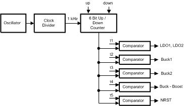 Figure 66. Power Sequencer Block Diagram
8.4.2.2 Power-On Timing
Each timeout T1 thru to T5 are factory programmed from 0 ms to 63 ms. The power-on defaults are shown in Table 9.
Table 9. Power-On Timing Defaults
| SYMBOL | DESCRIPTION | TIME (STANDARD OPTIONS) | TIME (AP OPTION) | UNIT |
|---|---|---|---|---|
| T1 | Delay for LDO1 and LDO2 | 5 | 6 | ms |
| T2 | Delay to Buck1 | 15 | 3 | ms |
| T3 | Delay for Buck2 | 20 | 1 | ms |
| T4 | Delay for Buck-Boost | 25 | 0 | ms |
| T5 | Delay for NRST | 60 | 10 | ms |
8.4.2.3 Power-Off Timing
The timing delays during a power-off sequence are equal to 63 ms minus the timing delay during the power on sequence (see Table 10).
Table 10. Power-Off Timing Defaults
| SYMBOL | DESCRIPTION | TIME (STANDARD OPTIONS) | TIME (AP option) | UNIT |
|---|---|---|---|---|
| T1 | Delay for LDO1 and LDO2 | 58 | 10 | ms |
| T2 | Delay to Buck1 | 48 | 10 | ms |
| T3 | Delay for Buck2 | 43 | 10 | ms |
| T4 | Delay for Buck-Boost | 38 | 10 | ms |
| T5 | Delay for NRST | 3 | 3 | ms |
8.4.2.4 Transitioning From Standby to Active Mode (Power Up) Battery Power Present Only
When only battery power is present and the battery voltage VBATT > VBATTLOW, the LP3910 is waiting for one of three valid wakeup signals. The first is the ONOFF pin. The second and third wakeups are the wall adapter and USBPWR. The ONOFF pin is a factory-programmable wakeup source. It can be a rising edge, a falling edge, a level high, or a level low event. Regardless of the mode, the signal requires a 32-ms deglitch time. A deglitched version of the ONOFF pin is output on the open-drain output pin ONSTAT. ONOFF is usually connected to a push button. Asserting the ONOFF pin starts the power-on sequencer. This enables the DC-DC converters, including the Buck1 DC-DC converter that supplies power to the system processor. The system processor then must set bit D4 (PACK bit) in the power-on event register through the I2C interface or apply a logic high to the POWERACK pin to keep the device in the Active mode. These serve as power acknowledgment, confirming the power-on request initiated by the ONOFF pin. If neither the PACK bit (D4) in the PON register or the POWERACK pin is set within 128 ms (maximum) of the start of the power-up sequencer, the LP3910 is automatically turned off, as the system has failed to acknowledge the power-on request. Connecting the battery is considered a power-on event. However, hot insertion of the battery with the adapter connected is NOT permitted.
8.4.2.5 Transitioning From Active Mode to Standby Mode
8.4.2.5.1 External Event Triggers the Transition From Active to Standby Mode
When the device is active, a subsequent re-assertion of the push button turns off the LP3910 indirectly by first flagging the system processor though the ONSTAT pin. Upon detecting the ONSTAT transition, the system processor must clear bit D4 (PACK) in the power on event register and apply a logic low to the POWERACK pin to power down the LP3910, which then transitions to Standby Mode. Clearing the PACK register bit and POWERACK pin while external supply sources are present (either USB or CHG_IN) does not power down the LP3910, to keep the charger active. The system can as always disable all necessary DC-DC converters, except Buck1, through the register control.
When external power is disconnected, LP3910 remains in its active state unless the battery voltage is below VBLA (battery low alarm) or unless the PACK (either bit D4 in the PON register and the POWERACK pin) is cleared by the system processor.
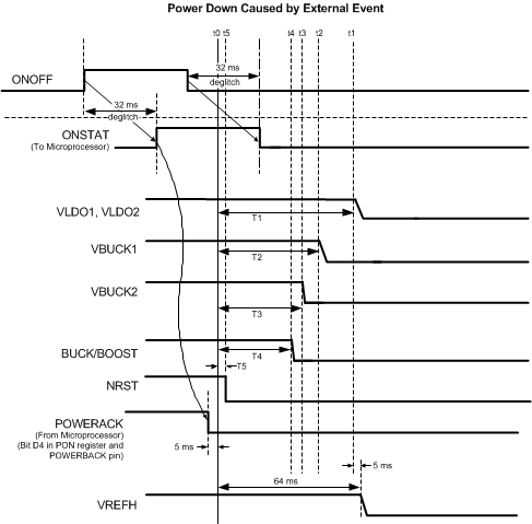 Figure 67. Power-Down Event Caused by External Event
8.4.2.5.2 Transition From Active to Standby Mode Due to Expiring POWERACK Deadline
With no external charger present when the system processor fails to acknowledge the power-on in time by setting either the PACK bit (D4) in the PON register or the POWERACK pin before the 128-ms deadline following the start of the power-up sequencer, then the NRST is immediately de-asserted and after 2 ms all power sources are disabled before transitioning to Standby Mode. This 2-ms delay allows the microprocessor to receive a clean reset before the power is de-asserted. A new power-on event is then required to transition back to active mode.
With either external charger present when the system processor fails to acknowledge the power-on in time by setting either the PACK bit (D4) in the PON register or the POWERACK pin before the 128-ms deadline following the start of the power-up sequencer, the NRST is immediately de-asserted; after 2 ms all power sources are disabled before transitioning to charger standby mode.
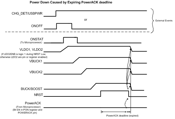 Figure 68. Power Down Caused by Expiring PowerACK Deadline
8.4.2.5.3 Transition From Charger Standby Mode to Either Active or Standby Mode
While in charger standby mode, the battery is charged using the default values of IPROG, EOC, VTERM, battery temperature range, and USB ISEL. In charger standby mode, all the regulators and the I2C are disabled. A new power-on event is required to transition back to active mode. Removing the charger during charger standby mode causes a transition back to standby mode.
8.5 Programming
8.5.1 I2C-Compatible Serial Interface
8.5.1.1 I2C Signals
The LP3910 features an I2C-compatible serial interface, using two dedicated pins: I2C_SCL and I2C_SDA for I2C clock and data, respectively. Both signals need a pullup resistor according to the I2C specification. The LP3910 interface is an I2C slave that is clocked by the incoming SCL clock.
Signal timing specifications are according to the I2C bus specification. The maximum bit rate is 400 kbit/s. See I2C specification from NXP for further details.
8.5.1.2 I2C Data Validity
The data on I2C_SDA line must be stable during the HIGH period of the clock signal (I2C_SCL); that is, the state of the data line can only be changed when CLK is LOW.
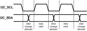 Figure 69. I2C Data Valid Diagram
8.5.1.3 I2C Start and Stop Conditions
START and STOP bits classify the beginning and the end of the I2C session. The START condition is defined the as the I2C_SDA signal transitioning from HIGH to LOW while SCL line is HIGH. The STOP condition is defined as the SDA transitioning from LOW to HIGH while I2C_SCL is HIGH. The I2C master always generates START and STOP bits. The I2C bus is considered to be busy after a START condition and free after a STOP condition. During data transmission, I2C master can generate repeated START conditions. First START and repeated START conditions are equivalent, function-wise.
 Figure 70. Start and Stop Conditions
8.5.1.4 Transferring Data
Every byte put on the I2C_SDA line must be eight bits long, with the most significant bit (MSB) being transferred first. Each byte of data has to be followed by an acknowledge bit. The acknowledged related clock pulse is generated by the master. The transmitter releases the I2C_SDA line (HIGH) during the acknowledge clock pulse. The receiver must pull down the I2C_SDA line during the 9th clock pulse, signifying acknowledgement. A receiver which has been addressed must generate an acknowledgement (ACK) after each byte has been received.
8.5.1.5 Register Write Cycle
After the START condition, the I2C master sends a chip address. This address is seven bits long followed by an eighth bit which is a data direction bit (R/W). For the eighth bit, a 0 indicates a WRITE, and a 1 indicates a READ. The second byte selects the register to which the data is written. The third byte contains data that is written to the selected register.
LP3910 has a chip address of 60’h, which is set by a metal mask option.
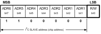 Figure 71. I2C Chip Address
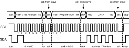
r = read (I2C_SDA = 1)
ack = acknowledge (I2C_SDA pulled down by either master or slave)
rs = repeated start
id = LP3910 chip address: 60’h
8.5.1.6 Register Read Cycle
When a READ function is to be accomplished, a WRITE function must precede the READ function, as shown Figure 73.
 Figure 73. I2C Read Cycle
8.5.1.7 Multi-Byte I2C Command Sequence
The I2C serial interface of the LP3910 device supports random register multi-byte command sequencing: during a multi-byte write the Master sends the Start command followed by the device address, which is sent only once, followed by the 8-bit register address, then 8 bits of data, The I2C slave must then accept the next random register address followed by 8 bits of data and continue this process until the master sends a valid stop condition.
A typical multi-byte random register transfer is: Device Address, Register A Address, Ack, Register A Data, Ack Register M Address, Ack, Register M Data, Ack Register X Address, Ack, Register X Data, Ack Register Z Address, Ack, Register Z Data, Ack, Stop
NOTE
The PMIC is not required to detect the I2C device address for each transaction. A, M, X, and Z are random numbers.
 Figure 74. Example Multi-Byte Command Sequencing
8.6 Register Maps
8.6.1 LDO1 Control Register
LDO1 can be configured through its own I2C control register. The output voltage is programmable in steps of 100 mV from 1.2 V to 3.3 V. LDO1 gets enabled during the power-on sequence. Disable/enable control is provided through bit D5 in the LDO1 control register after selecting the appropriate D4–0 settings, which determine the output voltage.
The output voltage can be altered while LDO1 is enabled. When LDO1 is disabled, it shunts the output to AGND with a RSHUNT = 200 Ω (maximum).
8.6.2 BATTLOW Register (04)H Battery Low Alarm Register
| D7–5 | D4–0 | |||
| Access | Read Only 0 | R/W | ||
| Data | Reserved | Battery low threshold voltage (V) | Battery low IRQ threshold voltage (V) | |
| 5’h14–1F | 2.50 | 2.70 | ||
| 5’h13 | 2.55 | 2.75 | ||
| 5’h12 | 2.60 | 2.80 | ||
| 5’h11 | 2.65 | 2.85 | ||
| 5’h10 | 2.70 | 2.90 | ||
| 5’h0F | 2.75 | 2.95 | ||
| 5’h0E | 2.80 | 3.00 | ||
| 5’h0D | 2.85 | 3.05 | ||
| 5'h0C | 2.90 | 3.10 | ||
| 5’h0B | 2.95 | 3.15 | ||
| 5’h0A | 3.00 | 3.20 | ||
| 5’h09 | 3.05 | 3.25 | ||
| 5’h08 | 3.10 | 3.30 | ||
| 5’h07 | 3.15 | 3.35 | ||
| 5’h06 | 3.20 | 3.40 | ||
| 5’h05 | 3.25 | 3.45 | ||
| 5’h04 | 3.30 | 3.50 | ||
| 5’h03 | 3.35 | 3.55 | ||
| 5’h02 | 3.40 | 3.60 | ||
| 5’h01 | 3.45 | 3.65 | ||
| 5’h00 | 3.50 | 3.70 | ||
| Reset Standard Default “AP” Default |
n/a |
5’h0C 5’h1F |
2.90 2.70 |
3.10 2.70 |
8.6.3 PON Register (00)H Power-On Event Register
| D7–5 | D4 | D3 | D2 | D1 | D0 | |
| Access | Read Only 0 | R/W | Read Only | |||
| Data | Reserved | PACK | Battery Insert | PON by ONOFF | PON by CHG_IN | PON by USB Power |
| 0: Disable Power, go in standby, and wait for power on event. | 0: default | 0: default | 0: default | 0: default | ||
| 1: Acknowledge Power On request | 1: Battery Insert caused by Battery Insertion | 1: ONOFF caused Power On event | 1: Power On caused by CHG_IN power detection | 1: Power On caused by USB power detection | ||
| Reset | n/a | 0 | 0 | 0 | 0 | 0 |
8.6.4 CHCTL Register (01)H Charger Control Register
| D7–6 | D5–2 | D1 | D0 | |
| Access | R/W | |||
| Data | Termination voltage | ICC: Full Rate Charge current | Charger enable | End of Charge Select |
| 00: 4.1V (Li Ion) 01: 4.2V (Li Polymer ) 10: 4.38V (Li Polymer) 11: reserved |
0000: 100 mA 0001: 200 mA 0010: 300 mA 0011: 400 mA 0100: 500 mA 0101: 600 mA 0110: 700 mA 0111: 800 mA 1000: 900 mA 1001: 1000 mA |
0: disabled 1: enabled |
0: 5% 1: 10% |
|
| Reset | 01 | Factory-Programmed Default | 1 | 1 |
8.6.5 CHSPV Register (02)H Charger Supervisor Register
| D7–6 | D5 | D4 | D3 | D2–0 | ||||
| Access | Read only | R/W | R/W | R/W | ||||
| Data | Reserved | LED Current | LED ENABLE
0: Disabled 1:Enabled |
Battery temperature range | Charger status | |||
| 0: 5 mA (Standard default) 0: 1 mA (AP default) |
0: 0°C–50°C | Stat2 | Stat1 | Stat0 | ||||
| 1: 10 mA (Standard default) 1: 2 mA (AP default) |
1: 0°C–45°C | 0 | 0 | 0 | Charger is off | |||
| 0 | 0 | 1 | Prequalification | |||||
| 0 | 1 | 0 | Constant current charging | |||||
| 0 | 1 | 1 | Constant voltage charging | |||||
| 1 | 0 | 0 | Error | |||||
| 1 | 0 | 1 | Charge cycle complete | |||||
| 1 | 1 | 0 | Safety Timer Expired | |||||
| 1 | 1 | 1 | EOC / Top-off | |||||
| Reset | n/a | 1 | 1 | 0 | 2’b000 | |||
8.6.6 ILIMIT Register (03)H Current Limit Register
| D7–2 | D1–0 | |
| Access | Read only 0 | |
| Data | Reserved | USB Current Limit |
| 00: controlled by USBISEL pin [low = 100 mA, high = 500 mA] 01: 100 mA 10: 500 mA 11: 800 mA |
||
| Reset | n/a | 2’b00 |
8.6.7 ADCC Register (0a)H ADC Control Register
| D7 | D6 | D5 | D4 | D3 | D2 | D1–0 | |
| Access | R/W | R/W | Read Only | R/W | R/W | ||
| Data | VRANGE | IRANGE | ADC Overflow | Data Ready | Start Conversion | ADC Enable | ADC source selection |
| 0: 2.6 V – 3.5 V | 0: 0 mA – 605 mA | 0: no overflow | 0: no data | 0: default | 0: Disabled | 00: battery voltage | |
| 1: 2.6 V – 4.4 V | 1: 0 mA – 1100 mA | 1: overflow | 1: data ready | 1: start conversion | 1: Enabled | 01: battery charge current | |
| 10: ADC1 | |||||||
| 11: ADC2 | |||||||
| Reset | 0 | 0 | 0 | 0 | 0 | 0 | 0 |
8.6.8 ADCD Register (0b)H ADC Output Data Register
Charge current 0 A to 1.1 A mirrored to 0 µA to 250 µA, ADC measures voltage drop across RSENSE 4.64 kΩ.
| D7–0 | |||
| Access | Read Only 0 | ||
| Data | Battery voltage: | 8’h00 = 2.6V | 8’hFF = 3.5V 1 LSB = 0.9 / 256 = (3.5 mV) range 0 |
| 8’h00= 2.6V | 8’hFF = 4.4 V 1 LSB = 1.8 / 256 = (7.0 mV) range 1 | ||
| Battery charge current | 8’h00 = 0 | 8’hFF = 0.6463 V = 605 mA range 0 | |
| 8’h00 = 0 | 8’hFF = 1.175V = 1100 mA range 1 | ||
| ADC1: 8’h00 = VREFH = 1.225V 8’hFF = 2*VREFH = 2.45 V (1 LSB = VREFH/256) | |||
| ADC2: 8’h00 = VREFH = 1.225V 8’hFF = 2*VREFH = 2.45 V (1 LSB = VREFH/256) | |||
| Reset | 8’h00 | ||
8.6.9 IMR Register (0c)H Interrupt Mask Register
| D7–0 | |
| Access | r/w |
| Data | 1: Enable INTn (n=0…7) to pull IRQB low 0: Mask Interrupt source INTn |
| Reset | 8’h00 |
8.6.10 IRQ Register (0d)H Interrupt Request Register
| D7–0 | |
| Access | Read only |
| Data | 1: Interrupt IRQn (n=0…7) requested 0: No interrupt requested |
| Reset | 8’h00 |
8.6.11 LDO1 Control Register (08)H
| D7–6 | D5 | D4–0 | ||
| Access | Read Only 0 | R/W | ||
| Data | Reserved | Operation
0: disable 1: enable |
LDO1 Output Voltage (V) | |
| 5’h00 | 1.2 | |||
| 5’h01 | 1.3 | |||
| 5’h02 | 1.4 | |||
| 5’h03 | 1.5 | |||
| 5’h04 | 1.6 | |||
| 5’h05 | 1.7 | |||
| 5’h06 | 1.8 | |||
| 5’h07 | 1.9 | |||
| 5’h08 | 2.0 | |||
| 5’h09 | 2.1 | |||
| 5’h0A | 2.2 | |||
| 5’h0B | 2.3 | |||
| 5’h0C | 2.4 | |||
| 5’h0D | 2.5 | |||
| 5’h0E | 2.6 | |||
| 5’h0F | 2.7 | |||
| 5’h10 | 2.8 | |||
| 5’h11 | 2.9 | |||
| 5’h12 | 3.0 | |||
| 5’h13 | 3.1 | |||
| 5’h14 | 3.2 | |||
| 5’h15 –5’h1F | 3.3 | |||
| Reset | n/a | 1 | Factory-Programmed Default | |
8.6.12 LDO2 Control Register
LDO2 can be configured through its own I2C control register. The output voltage is programmable in steps of 100 mV from 1.3 V to 3.3 V. LDO2 is by default disabled and can be enabled by setting bit D5 in the control register after selecting the appropriate D4–0 settings, which determine the output voltage. LDO2 can also be enabled through the external LDO2EN pin, which is the default enable control. With a logic 0 programmed to bit D5 in the corresponding control register, enable/disable control is passed onto the LDO2EN pin; a logic 1 applied to this pin enables LDO2 while a logic 0 disables the LDO2. Setting D5 to 1 in the LDO2 control register enables LDO2, regardless of the state of the LDO2EN pin. If the system designer permanently connects the LDO2EN pin to GND, then D5 is simply a enable/disable control bit. If the system design permanently connects the LDO2EN pin to VDD, the LDO is enabled during the power-on sequence and is always on, regardless of the state of bit D5 in the LDO2 control register. In that particular case, the LDO2 is sequenced with the same timing as LDO1 (see Power-On, Power-Off Sequencing).
The output voltage can be altered while LDO2 is enabled. When LDO2 is disabled, it shunts the output to AGND with a RSHUNT = 200 Ω (maximum).
Table 11. LDO2 Control Register (09)H
| D7–6 | D5 | D4–0 | ||
| Access | Read Only 0 | R/W | ||
| Data | Reserved | Operation
0: enable/ disable determined by state of LDO2EN pin 1: enable, override LDO2EN state |
LDO1 Output Voltage (V) | |
| 5’h00 | 1.3 | |||
| 5’h01 | 1.4 | |||
| 5’h02 | 1.5 | |||
| 5’h03 | 1.6 | |||
| 5’h04 | 1.7 | |||
| 5’h05 | 1.8 | |||
| 5’h06 | 1.9 | |||
| 5’h07 | 2 | |||
| 5’h08 | 2.1 | |||
| 5’h09 | 2.2 | |||
| 5’h0A | 2.3 | |||
| 5’h0B | 2.4 | |||
| 5’h0C | 2.5 | |||
| 5’h0D | 2.6 | |||
| 5’h0E | 2.7 | |||
| 5’h0F | 2.8 | |||
| 5’h10 | 2.9 | |||
| 5’h11 | 3 | |||
| 5’h12 | 3.1 | |||
| 5’h13 | 3.2 | |||
| 5’h14 –5’h1F | 3.3 | |||
| Reset | n/a | 0 | Factory-Programmed Default | |
8.6.13 Buck1, Buck2 Control Registers and BUCK1EN Pin
Buck1 and Buck2 are configurable through I2C accessible registers. Bit fields D4–0 control the output voltage. Bit D5 defines the Modulation mode of the buck, which by default automatically selects PWM or PFM mode depending on the load as described above in the functional description. The modulation mode can be forced to PWM mode regardless of the load by setting bit D5 to a logic 1 in the corresponding buck control register.
Bit D6 controls the enable/disable state of the buck, which is different for Buck1 and Buck2 as Buck1 has an external enable pin: BUCK1EN.
For Buck1, by default or when D6 is programmed logic 0 in the Buck1 control register, enable/disable control is passed onto the BUCK1EN pin. A logic 1 applied to this pin enables Buck1 while a logic 0 disables Buck1. Setting D6 to 1 in the Buck1 control register enables BUCK1, regardless of the state of the BUCK1EN pin. If the system designer permanently connects the BUCK1EN pin to GND, then D6 is simply a enable/disable control bit. If the system design permanently connects the enable pin to VDD, then the Buck1 is enabled during the power-on sequence and is always be on, regardless of the state of bit D6 in the Buck1 control register (see Power-On, Power-Off Sequencing).
BUCK2 is by default enabled during the power-on sequence and can be enabled/disabled through bit D6 in the Buck2 control register.
Table 12. Buck1 Control Register (05)H
| D7 | D6 | D5 | D4–0 | ||
| Access | Read Only 0 | R/W | |||
| Data | Reserved | Operation
0: enable/disable determined by state of BUCK1EN pin 1: enable, override BUCK1EN state |
Force PWM mode
0: Automatic Modulation Mode 1: Force PWM mode |
BUCK1 Output Voltage (V) | |
| 5’h00 | Externally controlled | ||||
| 5’h01 | 0.80 | ||||
| 5’h02 | 0.85 | ||||
| 5’h03 | 0.90 | ||||
| 5’h04 | 0.95 | ||||
| 5’h05 | 1.00 | ||||
| 5’h06 | 1.05 | ||||
| 5’h07 | 1.10 | ||||
| 5’h08 | 1.15 | ||||
| 5’h09 | 1.20 | ||||
| 5’h0A | 1.25 | ||||
| 5’h0B | 1.30 | ||||
| 5’h0C | 1.35 | ||||
| 5’h0D | 1.40 | ||||
| 5’h0E | 1.45 | ||||
| 5’h0F | 1.50 | ||||
| 5’h10 | 1.55 | ||||
| 5’h11 | 1.60 | ||||
| 5’h12 | 1.65 | ||||
| 5’h13 | 1.70 | ||||
| 5’h14 | 1.75 | ||||
| 5’h15 | 1.80 | ||||
| 5’h16 | 1.85 | ||||
| 5’h17 | 1.90 | ||||
| 5’h18 | 1.95 | ||||
| 5’h19–1F | 2.00 | ||||
| Reset | n/a | 0 | 0 | Factory-Programmed Default | |
Table 13. Buck2 Control Register (06)H
| D7 | D6 | D5 | D4–0 | ||
| Access | Read Only 0 | R/W | |||
| Data | Reserved | Operation
0: disabled 1: enabled |
Force PWM mode
0: Automatic Modulation Mode 1: Force PWM mode |
BUCK2 Output Voltage (V) | |
| 5’h00 | Externally controlled | ||||
| 5’h01 | 1.80 | ||||
| 5’h02 | 1.90 | ||||
| 5’h03 | 2.00 | ||||
| 5’h04 | 2.10 | ||||
| 5’h05 | 2.20 | ||||
| 5’h06 | 2.30 | ||||
| 5’h07 | 2.40 | ||||
| 5’h08 | 2.50 | ||||
| 5’h09 | 2.60 | ||||
| 5’h0A | 2.70 | ||||
| 5’h0B | 2.80 | ||||
| 5’h0C | 2.90 | ||||
| 5’h0D | 3.00 | ||||
| 5’h0E | 3.10 | ||||
| 5’h0F | 3.20 | ||||
| 5’h1x | 3.30 | ||||
| Reset | n/a | 1 | 0 | Factory-Programmed Default | |
8.6.14 Buck-Boost Control Register
The buck-boost is controlled through its dedicated control register. The buck-boost is enabled through the power-on sequencing. The system processor is required to select the desired buck-boost output voltage through bits D4–0 before enabling it by setting bit D6 in the control register. The buck-boost is also disabled when b’00000 is programmed in the register field D4–0, regardless of the state of the bit D6. When the buck-boost is disabled, its output is internally tied low through a 1-MΩ resistor. If D4–0 is set to b’00000 the 1 MΩ resistor is disconnected. The default output voltage for the buck-boost is factory programmable.
Table 14. Buck–Boost Control Register (07)H
| D7 | D6 | D5 | D4–0 | ||
| Access | Read Only 0 | R/W | |||
| Data | Reserved | Force PWM
0: Automatic modulation mode 1: Force PWM modulation |
Operation
0: disable 1: enable |
Buck–Boost Output Voltage (V) | |
| 5’h00 | disabled | ||||
| 5’h01 | 1.80 | ||||
| 5’h02 | 1.85 | ||||
| 5’h03 | 1.90 | ||||
| 5’h04 | 1.95 | ||||
| 5’h05 | 2.00 | ||||
| 5’h06 | 2.05 | ||||
| 5’h07 | 2.10 | ||||
| 5’h08 | 2.15 | ||||
| 5’h09 | 2.20 | ||||
| 5’h0A | 2.25 | ||||
| 5’h0B | 2.30 | ||||
| 5’h0C | 2.35 | ||||
| 5’h0D | 2.40 | ||||
| 5’h0E | 2.45 | ||||
| 5’h0F | 2.50 | ||||
| 5’h10 | 2.55 | ||||
| 5’h11 | 2.60 | ||||
| 5’h12 | 2.65 | ||||
| 5’h13 | 2.70 | ||||
| 5’h14 | 2.75 | ||||
| 5’h15 | 2.80 | ||||
| 5’h16 | 2.85 | ||||
| 5’h17 | 2.90 | ||||
| 5’h18 | 2.95 | ||||
| 5’h19 | 3.00 | ||||
| 5’h1A | 3.05 | ||||
| 5’h1B | 3.10 | ||||
| 5’h1C | 3.15 | ||||
| 5’h1D | 3.20 | ||||
| 5’h1E | 3.25 | ||||
| 5’h1F | 3.30 | ||||
| Reset | n/a | 0 | 1 | Factory-Programmed Default | |