SNVS159H October 2001 – July 2015 LP3981
PRODUCTION DATA.
- 1 Features
- 2 Applications
- 3 Description
- 4 Revision History
- 5 Pin Configuration and Functions
- 6 Specifications
- 7 Parameter Measurement Information
- 8 Detailed Description
- 9 Application and Implementation
- 10Power Supply Recommendations
- 11Layout
- 12Device and Documentation Support
- 13Mechanical, Packaging, and Orderable Information
Package Options
Mechanical Data (Package|Pins)
Thermal pad, mechanical data (Package|Pins)
Orderable Information
8 Detailed Description
8.1 Overview
The LP3981 family of fixed-output, ultra-low-dropout, and low-noise regulators offers exceptional performance for battery-powered applications. Available for voltages from 2.5-V to 3.3-V, the family is capable of delivering
300-mA continuous load current.
The LP3981 contains several features to facilitate battery-powered designs:
- Low dropout voltage , typical dropout of 132-mV at 300-mA load current.
- Low quiescent current and low ground current. Ground current is typically 170 µA at 150-mA load, and 70 µA at 1-mA load.
- A shutdown feature is available , allowing the regulator to consume only 0.003 µA typically when the EN pin is pulled low.
- Power supply rejection is 60-dB at 1 kHZ.
- Low noise; BYPASS pin allows for low-noise operation, with typically 35-µVRMS output noise over 10 Hz to 100 kHz.
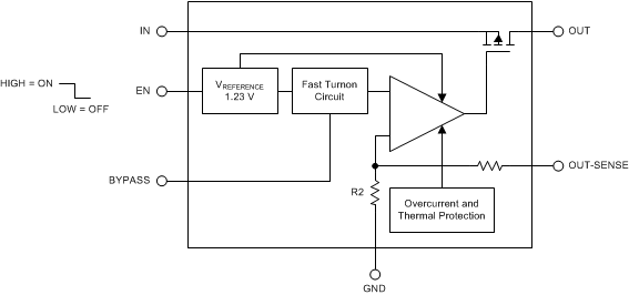
8.2 Functional Block Diagram

8.3 Feature Description
8.3.1 On/Off Input Operation
The LP3981 is turned off by pulling the EN pin low, and turned on by pulling it high. If this feature is not used, the EN pin must be tied to VIN to keep the regulator output on at all time. To assure proper operation, the signal source used to drive the EN input must be able to swing above and below the specified turnon and turnoff voltage thresholds listed in Electrical Characteristics under VIL and VIH.
8.4 Device Functional Modes
8.4.1 Operation with VOUT(TARGET) + 0.3 V ≤ VIN ≤ 6 V
The device operate if the input voltage is equal to, or exceeds VOUT(TARGET) + 0.3 V. At input voltages below the minimum VIN requirement, the devices do not operate correctly and output voltage may not reach target value.
8.4.2 Operation With EN Control
If the voltage on the EN pin is less than 0.4 V, the device is disabled, and in this state the shutdown current does not exceed 1.5 μA. Raising EN above 1.4 V initiates the start-up sequence of the device.