SNVS159H October 2001 – July 2015 LP3981
PRODUCTION DATA.
- 1 Features
- 2 Applications
- 3 Description
- 4 Revision History
- 5 Pin Configuration and Functions
- 6 Specifications
- 7 Parameter Measurement Information
- 8 Detailed Description
- 9 Application and Implementation
- 10Power Supply Recommendations
- 11Layout
- 12Device and Documentation Support
- 13Mechanical, Packaging, and Orderable Information
Package Options
Mechanical Data (Package|Pins)
Thermal pad, mechanical data (Package|Pins)
Orderable Information
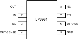
5 Pin Configuration and Functions
DGK Package
8-Pin VSSOP
Top View

NGC Package
6-Pin WSON With Exposed Thermal Pad
Top View

Pin Descriptions
| PIN | TYPE | DESCRIPTION | ||
|---|---|---|---|---|
| NAME | VSSOP | WSON | ||
| BYPASS | 6 | 5 | — | Optional bypass capacitor for noise reduction. |
| EN | 7 | 6 | I | Enable input logic, enable high. |
| GND | 5 | 4 | G | Common ground. Connect to PAD. |
| IN | 2 | 2 | I | Input voltage of the LDO. |
| NC | 3, 8 | — | — | No internal connection. |
| OUT | 1 | 1 | O | Output voltage of the LDO. |
| OUT-SENSE | 4 | 3 | O | Output. Voltage sense pin. Must be connected to OUT for proper operation. |
| THERMAL PAD | — | √ | — | Common ground. Connect to pin 4. |