SNVS087AE October 2000 – May 2015 LP3985
PRODUCTION DATA.
- 1 Features
- 2 Applications
- 3 Description
- 4 Revision History
- 5 Pin Configuration and Functions
- 6 Specifications
- 7 Detailed Description
- 8 Application and Implementation
- 9 Power Supply Recommendations
- 10Layout
- 11Device and Documentation Support
- 12Mechanical, Packaging, and Orderable Information
Package Options
Mechanical Data (Package|Pins)
Thermal pad, mechanical data (Package|Pins)
Orderable Information
10 Layout
10.1 Layout Guidelines
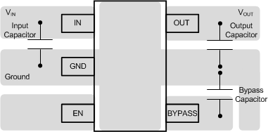
For best overall performance, place all circuit components on the same side of the circuit board and as near as practical to the respective LDO pin connections. Place ground return connections to the input and output capacitor, and to the LDO ground pin as close to each other as possible, connected by a wide, component-side, copper surface. The use of vias and long traces to create LDO circuit connections is strongly discouraged and negatively affects system performance. This grounding and layout scheme minimizes inductive parasitics, and thereby reduces load-current transients, minimizes noise, and increases circuit stability. A ground reference plane is also recommended and is either embedded in the PCB itself or located on the bottom side of the PCB opposite the components. This reference plane serves to assure accuracy of the output voltage, shield noise, and behaves similar to a thermal plane to spread (or sink) heat from the LDO device. In most applications, this ground plane is necessary to meet thermal requirements.
10.2 Layout Examples
 Figure 41. LP3985 SOT-23 Package Typical Layout
 Figure 42. LP3985 DSBGA Package Typical Layout
10.3 DSBGA Mounting
The DSBGA package requires specific mounting techniques which are detailed in Texas Instruments Application Note 1112 DSBGA Wafer Level Chip Scale Package (SNVA009). Referring to the section Surface Mount Technology (SMT) Assembly Considerations, it should be noted that the pad style which must be used with the 5-bump package is NSMD (non-solder mask defined) type.
For best results during assembly, alignment ordinals on the PC board may be used to facilitate placement of the DSBGA device.
10.4 DSBGA Light Sensitivity
Exposing the DSBGA device to direct sunlight will cause mis-operation of the device. Light sources such as halogen lamps can effect electrical performance if brought near to the device.
The wavelengths which have most detrimental effect are reds and infra-reds, which means that the fluorescent lighting used inside most buildings has very little effect on performance. A DSBGA test board was brought to within 1 cm of a fluorescent desk lamp and the effect on the regulated output voltage was negligible, showing a deviation of less than 0.1% from nominal.