SLAS928B March 2013 – November 2016 LP3988-Q1
PRODUCTION DATA.
- 1 Features
- 2 Applications
- 3 Description
- 4 Revision History
- 5 Pin Configuration and Functions
- 6 Specifications
- 7 Parameter Measurement Information
- 8 Detailed Description
- 9 Application and Implementation
- 10Power Supply Recommendations
- 11Layout
- 12Device And Documentation Support
- 13Mechanical, Packaging, And Orderable Information
Package Options
Refer to the PDF data sheet for device specific package drawings
Mechanical Data (Package|Pins)
- DBV|5
Thermal pad, mechanical data (Package|Pins)
Orderable Information
1 Features
- Qualified for Automotive Applications
- AEC-Q100 Qualified With the Following Results:
- Device Temperature Grade 1: –40°C to +125°C Ambient Operating Temperature
- Device HBM ESD Classification Level H2
- Device CDM ESD Classification Level C4B
- Operating Input Voltage 2.5 V to 6 V
- Power-Good Flag Output
- Logic-Controlled Enable
- Stable With Ceramic and High-Quality Tantalum Capacitors
- Fast Turnon
- Thermal Shutdown and Short-Circuit Current Limit
- 5-Pin SOT-23 Package
2 Applications
- Automotive
- CDMA Cellular Handsets
- Wideband CDMA Cellular Handsets
- GSM Cellular Handsets
- Portable Information Appliances
3 Description
The LP3988-Q1 is a 150-mA low-dropout regulator designed specially to meet requirements of portable battery applications. The LP3988-Q1 works with a space-saving 1-µF ceramic capacitor. The LP3988-Q1 features an error flag-output that indicates a faulty output condition.
The LP3988-Q1 has performance optimized for battery-powered systems to deliver low noise, extremely low dropout voltage, and low quiescent current. Regulator ground current increases only slightly in dropout, further prolonging the battery life.
Power-supply rejection is better than 60 dB at low frequencies and starts to roll off at 10 kHz. The device maintains high power-supply rejection down to lower input voltage levels common to battery-operated circuits.
The device is ideal for mobile phone and similar battery-powered wireless applications. It provides up to 150 mA, from a 2.5-V to 6-V input, consuming less than 1 µA in disable mode, and has fast turnon time less than 200 µs.
The LP3988-Q1 is available in a 5-pin SOT-23 package, has performance specified for the −40°C to +125°C temperature range, and is available in a 2.85-V output voltage. For other voltage options, contact TI sales.
Device Information(1)
| PART NUMBER | PACKAGE | BODY SIZE (NOM) |
|---|---|---|
| LP3988-Q1 | SOT-23 (5) | 2.90 mm × 1.60 mm |
- For all available packages, see the orderable addendum at the end of the data sheet.
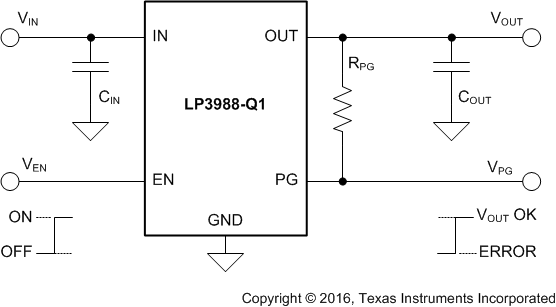
Simplified Schematic
