SLAS928B March 2013 – November 2016 LP3988-Q1
PRODUCTION DATA.
- 1 Features
- 2 Applications
- 3 Description
- 4 Revision History
- 5 Pin Configuration and Functions
- 6 Specifications
- 7 Parameter Measurement Information
- 8 Detailed Description
- 9 Application and Implementation
- 10Power Supply Recommendations
- 11Layout
- 12Device And Documentation Support
- 13Mechanical, Packaging, And Orderable Information
Package Options
Refer to the PDF data sheet for device specific package drawings
Mechanical Data (Package|Pins)
- DBV|5
Thermal pad, mechanical data (Package|Pins)
Orderable Information
11 Layout
11.1 Layout Guidelines
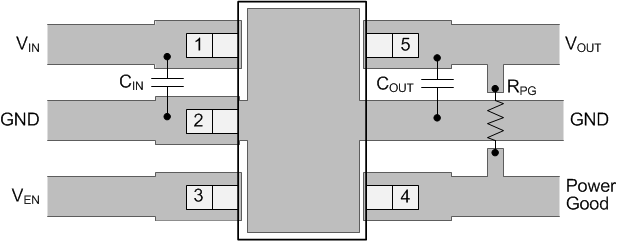
The dynamic performance of the LP3988-Q1 is dependant on the layout of the PCB. PCB layout practices that are adequate for typical LDOs may degrade the PSRR, noise, or transient performance of the LP3988-Q1.
Best performance is achieved by placing CIN and COUT on the same side of the PCB as the LP3988-Q1 device, and as close as is practical to the package. The ground connections for CIN and COUT must be back to the LP3988-Q1 GND pin using as wide and as short of a copper trace as is practical.
Avoid connections using long trace lengths, narrow trace widths, and/or connections through vias. These add parasitic inductances and resistance that results in inferior performance especially during transient conditions.
The PG pin pullup resistor must be connected to the LP3988-Q1 OUT pin, with the pullup resistor located as close as is practical to the PG pin.
11.2 Layout Example
 Figure 21. LP3988-Q1 SOT-23 Layout Example