SLAS928B March   2013  – November 2016 LP3988-Q1

PRODUCTION DATA.  

  1. Features
  2. Applications
  3. Description
  4. Revision History
  5. Pin Configuration and Functions
  6. Specifications
    1. 6.1 Absolute Maximum Ratings
    2. 6.2 ESD Ratings
    3. 6.3 Recommended Operating Conditions
    4. 6.4 Thermal Information
    5. 6.5 Electrical Characteristics
    6. 6.6 Timing Requirements
    7. 6.7 Typical Characteristics
  7. Parameter Measurement Information
  8. Detailed Description
    1. 8.1 Overview
    2. 8.2 Functional Block Diagram
    3. 8.3 Feature Description
      1. 8.3.1 Enable (En)
      2. 8.3.2 Regulated Output (OUT)
      3. 8.3.3 Power Good (PG) Output
      4. 8.3.4 PG Delay Time
      5. 8.3.5 Current Limit
      6. 8.3.6 Thermal Shutdown (TSD)
      7. 8.3.7 Fast Turnon Time
    4. 8.4 Device Functional Modes
      1. 8.4.1 Normal Operation
      2. 8.4.2 Dropout Operation
      3. 8.4.3 On/Off Input Operation
      4. 8.4.4 Disabled
  9. Application and Implementation
    1. 9.1 Application Information
    2. 9.2 Typical Application
      1. 9.2.1 Design Requirements
      2. 9.2.2 Detailed Design Procedure
        1. 9.2.2.1 External Capacitors
        2. 9.2.2.2 Input Capacitor
        3. 9.2.2.3 Output Capacitors
        4. 9.2.2.4 No-Load Stability
        5. 9.2.2.5 Capacitor Characteristics
        6. 9.2.2.6 Power Dissipation
        7. 9.2.2.7 Estimating Junction Temperature
      3. 9.2.3 Application Curves
  10. 10Power Supply Recommendations
  11. 11Layout
    1. 11.1 Layout Guidelines
    2. 11.2 Layout Example
  12. 12Device And Documentation Support
    1. 12.1 Related Documentation
    2. 12.2 Receiving Notification Of Documentation Updates
    3. 12.3 Community Resources
    4. 12.4 Trademarks
    5. 12.5 Electrostatic Discharge Caution
    6. 12.6 Glossary
  13. 13Mechanical, Packaging, And Orderable Information

Package Options

Refer to the PDF data sheet for device specific package drawings

Mechanical Data (Package|Pins)
  • DBV|5
Thermal pad, mechanical data (Package|Pins)
Orderable Information

Pin Configuration and Functions

DBV Package
5-Pin SOT-23
Top View
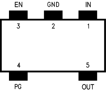
LP3988-Q1 20020507.png

Pin Functions

PIN TYPE DESCRIPTION
NAME NO.
EN 3 Input Enable input logic, enable high
GND 2 Ground Common ground
IN 1 Input Input voltage of the LDO
PG 4 Output Power Good flag (output): open-drain output, connected to an external pullup resistor. Active low indicates an output voltage out of tolerance condition.
OUT 5 Output Output voltage of the LDO