SNVS161E October   2001  – October 2015 LP3988

PRODUCTION DATA.  

  1. Features
  2. Applications
  3. Description
  4. Revision History
  5. Pin Configuration and Functions
  6. Specifications
    1. 6.1 Absolute Maximum Ratings
    2. 6.2 ESD Ratings
    3. 6.3 Recommended Operating Conditions
    4. 6.4 Thermal Information
    5. 6.5 Electrical Characteristics
    6. 6.6 Timing Requirements
    7. 6.7 Typical Characteristics
  7. Parameter Measurement Information
  8. Detailed Description
    1. 8.1 Overview
    2. 8.2 Functional Block Diagram
    3. 8.3 Feature Description
      1. 8.3.1 Enable (EN)
      2. 8.3.2 Regulated Output (OUT)
      3. 8.3.3 Power Good (PG) Output
      4. 8.3.4 PG Delay Time
      5. 8.3.5 Current Limit
      6. 8.3.6 Thermal Shutdown (TSD)
      7. 8.3.7 Fast Turnon Time
    4. 8.4 Device Functional Modes
      1. 8.4.1 Normal Operation
      2. 8.4.2 Dropout Operation
      3. 8.4.3 Disabled
  9. Application and Implementation
    1. 9.1 Application Information
    2. 9.2 Typical Application
      1. 9.2.1 Design Requirements
      2. 9.2.2 Detailed Design Procedure
        1. 9.2.2.1 External Capacitors
        2. 9.2.2.2 Input Capacitor
        3. 9.2.2.3 Output Capacitors
        4. 9.2.2.4 No-Load Stability
        5. 9.2.2.5 Capacitor Characteristics
        6. 9.2.2.6 Power Dissipation
        7. 9.2.2.7 Estimating Junction Temperature
      3. 9.2.3 Application Curves
  10. 10Power Supply Recommendations
  11. 11Layout
    1. 11.1 Layout Guidelines
    2. 11.2 Layout Examples
    3. 11.3 DSBGA Mounting
  12. 12Device and Documentation Support
    1. 12.1 Related Documentation
    2. 12.2 Community Resources
    3. 12.3 Trademarks
    4. 12.4 Electrostatic Discharge Caution
    5. 12.5 Glossary
  13. 13Mechanical, Packaging, and Orderable Information

Package Options

Mechanical Data (Package|Pins)
Thermal pad, mechanical data (Package|Pins)
Orderable Information

7 Parameter Measurement Information
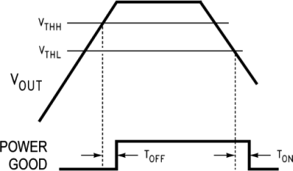
LP3988 20020522.png Figure 9. Power Good Flag Timing
LP3988 20020508.png Figure 10. Line Transient Response Input Perturbation
LP3988 20020509.png Figure 11. PSRR Input Perturbation