SNVSA66A October   2014  – December 2015 LP3990-Q1

PRODUCTION DATA.  

  1. Features
  2. Applications
  3. Description
  4. Revision History
  5. Pin Configuration and Functions
  6. Specifications
    1. 6.1 Absolute Maximum Ratings
    2. 6.2 ESD Ratings
    3. 6.3 Recommended Operating Conditions
    4. 6.4 Thermal Information
    5. 6.5 Electrical Characteristics
    6. 6.6 Output Capacitor, Recommended Specifications
    7. 6.7 Timing Requirements
    8. 6.8 Typical Characteristics
  7. Detailed Description
    1. 7.1 Overview
    2. 7.2 Functional Block Diagram
    3. 7.3 Feature Description
      1. 7.3.1 Enable (EN)
      2. 7.3.2 Thermal Overload Protection (TSD)
    4. 7.4 Device Functional Modes
      1. 7.4.1 Enable (EN)
      2. 7.4.2 Minimum Operating Input Voltage (VIN)
  8. Application and Implementation
    1. 8.1 Application Information
    2. 8.2 Typical Application
      1. 8.2.1 Design Requirements
      2. 8.2.2 Detailed Design Procedure
        1. 8.2.2.1 Power Dissipation and Device Operation
        2. 8.2.2.2 External Capacitors
        3. 8.2.2.3 Input Capacitor
        4. 8.2.2.4 Output Capacitor
        5. 8.2.2.5 No-Load Stability
        6. 8.2.2.6 Capacitor Characteristics
        7. 8.2.2.7 Enable Control
      3. 8.2.3 Application Curves
  9. Power Supply Recommendations
  10. 10Layout
    1. 10.1 Layout Guidelines
    2. 10.2 Layout Example
    3. 10.3 DSBGA Mounting
    4. 10.4 DSBGA Light Sensitivity
  11. 11Device and Documentation Support
    1. 11.1 Documentation Support
      1. 11.1.1 Related Documentation
    2. 11.2 Community Resources
    3. 11.3 Trademarks
    4. 11.4 Electrostatic Discharge Caution
    5. 11.5 Glossary
  12. 12Mechanical, Packaging, and Orderable Information

Package Options

Mechanical Data (Package|Pins)
Thermal pad, mechanical data (Package|Pins)
Orderable Information

5 Pin Configuration and Functions

DSBGA (YZR)
4 Pins
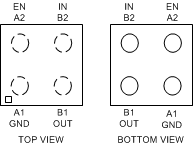
LP3990-Q1 connection_TL_snvs251.gif

Pin Functions

PIN I/O DESCRIPTION
NO. NAME
A1 GND Common ground.
A2 EN I Enable Input; Enables the regulator when ≥ 0.95 V.
Disables the Regulator when ≤ 0.4 V.
Enable Input has 1-MΩ (typical) pulldown resistor to GND.
B1 OUT O Voltage output. A 1-µF low-ESR capacitor must be connected to this pin. Connect this output to the load circuit.
B2 IN I Voltage supply Input. A 1-µF capacitor must be connected at this input.