SNVS296J December 2006 – June 2016 LP3991
PRODUCTION DATA.
- 1 Features
- 2 Applications
- 3 Description
- 4 Revision History
- 5 Pin Configuration and Functions
- 6 Specifications
- 7 Detailed Description
- 8 Application and Implementation
- 9 Power Supply Recommendations
- 10Layout
- 11Device and Documentation Support
- 12Mechanical, Packaging, and Orderable Information
Package Options
Mechanical Data (Package|Pins)
- YZR|4
Thermal pad, mechanical data (Package|Pins)
Orderable Information
8 Application and Implementation
NOTE
Information in the following applications sections is not part of the TI component specification, and TI does not warrant its accuracy or completeness. TI’s customers are responsible for determining suitability of components for their purposes. Customers should validate and test their design implementation to confirm system functionality.
8.1 Application Information
The LP3991 can provide 300-mA output current with 1.65-V to 4-V input. It is stable with a 2.2-μF or 4.7-µF ceramic output capacitor. An optional external bypass capacitor reduces the output noise without slowing down the load transient response. Typical output noise is 280 μVRMS at frequencies from 10 Hz to 100 kHz. Typical power supply rejection is 65 dB at 1 kHz.
8.2 Typical Application
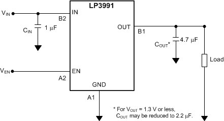 Figure 12. LP3991 Typical Application
8.2.1 Design Requirements
For typical linear voltage regulator applications, use the parameters listed in Table 2.
Table 2. Design Parameters
| DESIGN PARAMETER | EXAMPLE VALUE |
|---|---|
| Input voltage | 1.65 V to 4 V |
| Output voltage | 1.2 V to 2.8 V |
| Output current | 300 mA (maximum) |
| RMS noise, 10 Hz to100 kHz | 280 μVRMS |
| PSRR at 1 kHz | 65 dB |
8.2.2 Detailed Design Procedure
8.2.2.1 External Capacitors
In common with most regulators, the LP3991 requires external capacitors for regulator stability. The LP3991 is specifically designed for portable applications requiring minimum board space and smallest components. These capacitors must be correctly selected for good performance.
8.2.2.2 Input Capacitor
An input capacitor is required for stability. It is recommended that a 1-µF capacitor be connected between the LP3991 IN pin and ground (this capacitance value may be increased without limit).
This capacitor must be located a distance of not more than 1 cm from the IN pin and returned to a clean analog ground. Any good-quality ceramic, tantalum, or film capacitor may be used at the input.
NOTE
Tantalum capacitors can suffer catastrophic failures due to surge current when connected to a low-impedance source of power (like a battery or a very large capacitor). If a tantalum capacitor is used at the input, a surge current rating sufficient for the application must be ensured by the manufacturer.
There are no requirements for the equivalent series resistance (ESR) on the input capacitor, but tolerance, temperature, and voltage coefficients must be considered when selecting the capacitor to ensure the capacitance remains ≊ 1 µF over the entire operating temperature range.
8.2.2.3 Output Capacitor
Correct selection of the output capacitor is critical to ensure stable operation in the intended application.
The output capacitor must meet all the requirements specified in the recommended capacitor table over all conditions in the application. these conditions include DC bias, frequency and temperature. Unstable operation results if the capacitance drops below the minimum specified value.
The LP3991 is designed specifically to work with very small ceramic output capacitors. For voltage options of 1.5 V and higher, A 4.7-µF ceramic capacitor (dielectric type X7R or X5R) with an ESR between 5 mΩ to 500 mΩ, is suitable in the LP3991 application circuit. However, on lower VOUT options a 2.2-µF may be employed with only a small increase in load transient.
Other ceramic types such as Y5V and Z5U are less suitable owing to their inferior temperature characteristics. (See Capacitor Characteristics.)
It is also recommended that the output capacitor is placed within 1 cm of the OUT pin and returned to a clean, low impedance, ground connection.
It is possible to use tantalum or film capacitors at the device output, VOUT, but these are not as attractive for reasons of size and cost. (See Capacitor Characteristics.)
8.2.2.4 No-Load Stability
The LP3991 remains stable and in regulation with no external load. This is an important consideration in some circuits, for example CMOS RAM keep-alive applications.
8.2.2.5 Capacitor Characteristics
The LP3991 is designed to work with ceramic capacitors on the input and output to take advantage of the benefits they offer. For capacitance values around 4.7 µF, ceramic capacitors give the circuit designer the best design options in terms of low cost and minimal area.
For both input and output capacitors, careful interpretation of the capacitor specification is required to ensure correct device operation. The capacitor value can change greatly dependant on the conditions of operation and capacitor type.
In particular, to ensure stability, the output capacitor selection must take account of all the capacitor parameters, to ensure that the specification is met within the application. Capacitance value can vary with DC bias conditions as well as temperature and frequency of operation. Capacitor values also show some decrease over time due to aging. The capacitor parameters are also dependant on the particular case size with smaller sizes giving poorer performance figures in general.
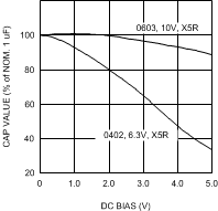 Figure 13. Effect of DC Bias on Capacitance Value
As an example Figure 13 shows a typical graph showing a comparison of capacitor case sizes in a capacitance vs. DC Bias plot. As shown in Figure 13, as a result of the DC Bias condition, the capacitance value may drop below the minimum capacitance value given in the recommended capacitor table. Note that Figure 13 shows the capacitance out of spec for the 0402 case size capacitor at higher bias voltages. TI therefore recommends that the capacitor manufacturers' specifications for the nominal value capacitor are consulted for all conditions as some capacitor sizes (for example, 0402) may not be suitable in the actual application. Ceramic capacitors have the lowest ESR values, thus making them best for eliminating high frequency noise. The ESR of a typical 4.7-µF ceramic capacitor is in the range of 20 mΩ to 40 mΩ, which easily meets the ESR requirement for stability for the LP3991. The temperature performance of ceramic capacitors varies by type. Capacitor type X7R is specified with a tolerance of ±15% over the temperature range –55°C to +125°C. The X5R has a similar tolerance over the reduced temperature range of –55°C to +85°C. Some large value ceramic capacitors (4.7 µF) are manufactured with Z5U or Y5V temperature characteristics, which can result in the capacitance dropping by more than 50% as the temperature varies from 25°C to +85°C. Therefore, X7R or X5R types are recommended in applications where the temperature changes significantly above or below 25°C.
Tantalum capacitors are less desirable than ceramic for use as output capacitors because they are more expensive when comparing equivalent capacitance and voltage ratings in the 1-µF to 4.7-µF range. Another important consideration is that tantalum capacitors have higher ESR values than equivalent size ceramics. This means that while it may be possible to find a tantalum capacitor with an ESR value within the stable range, it would have to be larger in capacitance (which means bigger and more costly) than a ceramic capacitor with the same ESR value. The ESR of a typical tantalum increases about 2:1 as the temperature goes from 25°C down to –40°C, so some guard band must be allowed.
8.2.2.6 Power Dissipation
Knowing the device power dissipation and proper sizing of the thermal plane connected to the tab or pad is critical to ensuring reliable operation. Device power dissipation depends on input voltage, output voltage, and load conditions and can be calculated with Equation 1.
Power dissipation can be minimized, and greater efficiency can be achieved, by using the lowest available voltage drop option that would still be greater than the dropout voltage (VDO). However, keep in mind that higher voltage drops result in better dynamic (that is, PSRR and transient) performance.
On the LP3991 DSBGA (YZR) package, the primary conduction path for heat is through the four bumps to the PCB. The maximum allowable junction temperature (TJ(MAX)) determines maximum power dissipation allowed (PD(MAX)) for the device package.
Power dissipation and junction temperature are most often related by the junction-to-ambient thermal resistance (RθJA) of the combined PCB and device package and the temperature of the ambient air (TA), according to Equation 2 or Equation 3:
Unfortunately, this RθJA is highly dependent on the heat-spreading capability of the particular PCB design, and therefore varies according to the total copper area, copper weight, and location of the planes. The RθJA recorded in Thermal Information is determined by the specific EIA/JEDEC JESD51-7 standard for PCB and copper-spreading area, and is to be used only as a relative measure of package thermal performance. For a well-designed thermal layout, RθJA is actually the sum of the package junction-to-board thermal resistance (RθJB) plus the thermal resistance contribution by the PCB copper area acting as a heat sink.
8.2.2.7 Estimating Junction Temperature
The EIA/JEDEC standard recommends the use of psi (Ψ) thermal characteristics to estimate the junction temperatures of surface mount devices on a typical PCB board application. These characteristics are not true thermal resistance values, but rather package specific thermal characteristics that offer practical and relative means of estimating junction temperatures. These psi metrics are determined to be significantly independent of copper-spreading area. The key thermal characteristics (ΨJT and ΨJB) are given in Thermal Information and are used in accordance with Equation 4 or Equation 5.
where
- PD(MAX) is explained in Equation 1
- TTOP is the temperature measured at the center-top of the device package.
where
- PD(MAX) is explained in Equation 1
- TBOARD is the PCB surface temperature measured 1 mm from the device package and centered on the package edge.
For more information about the thermal characteristics ΨJT and ΨJB, see Semiconductor and IC Package Thermal Metrics (SPRA953); for more information about measuring TTOP and TBOARD, see Using New Thermal Metrics (SBVA025); and for more information about the EIA/JEDEC JESD51 PCB used for validating RθJA, see the Thermal Characteristics of Linear and Logic Packages Using JEDEC PCB Designs (SZZA017). These application notes are available at www.ti.com.
8.2.3 Application Curves
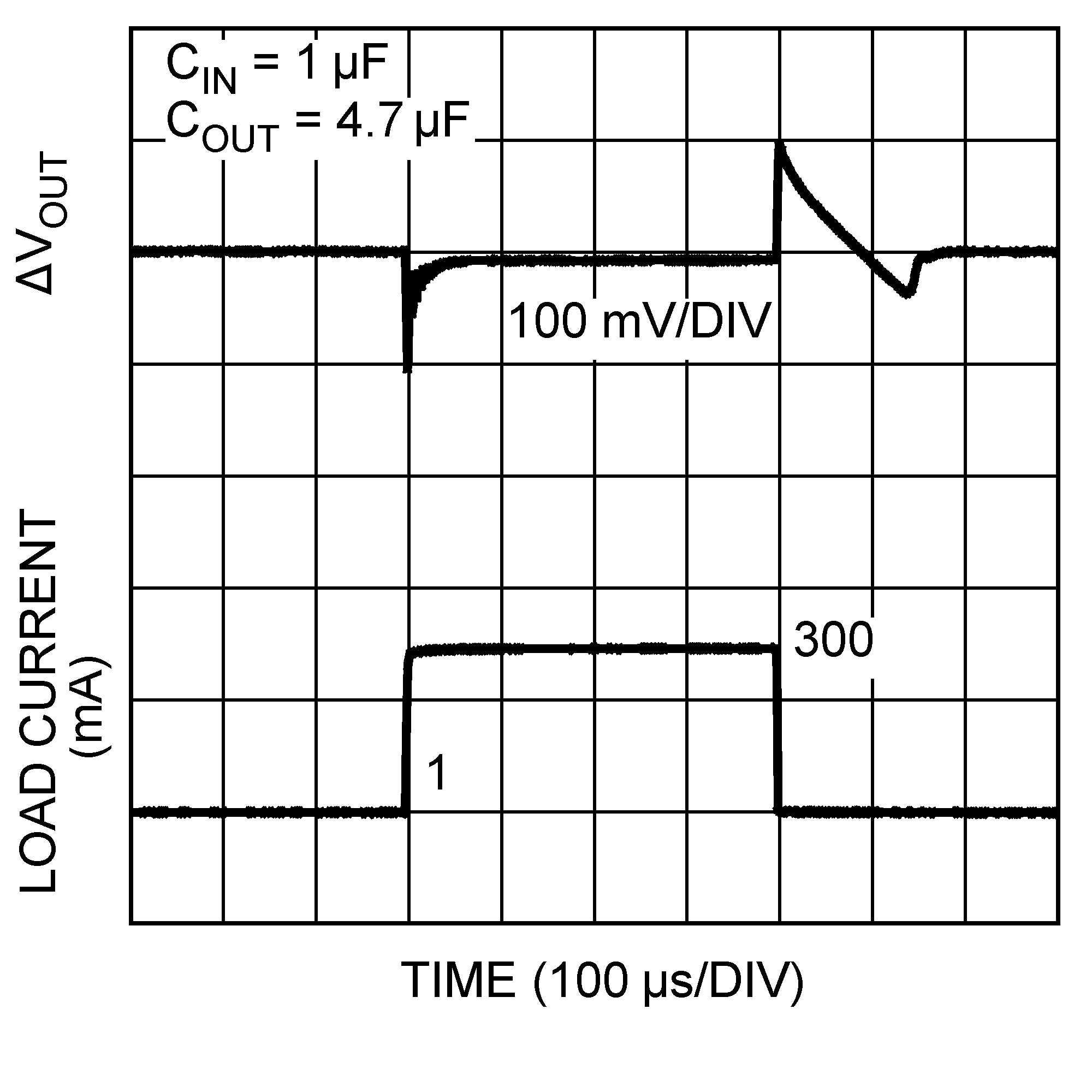
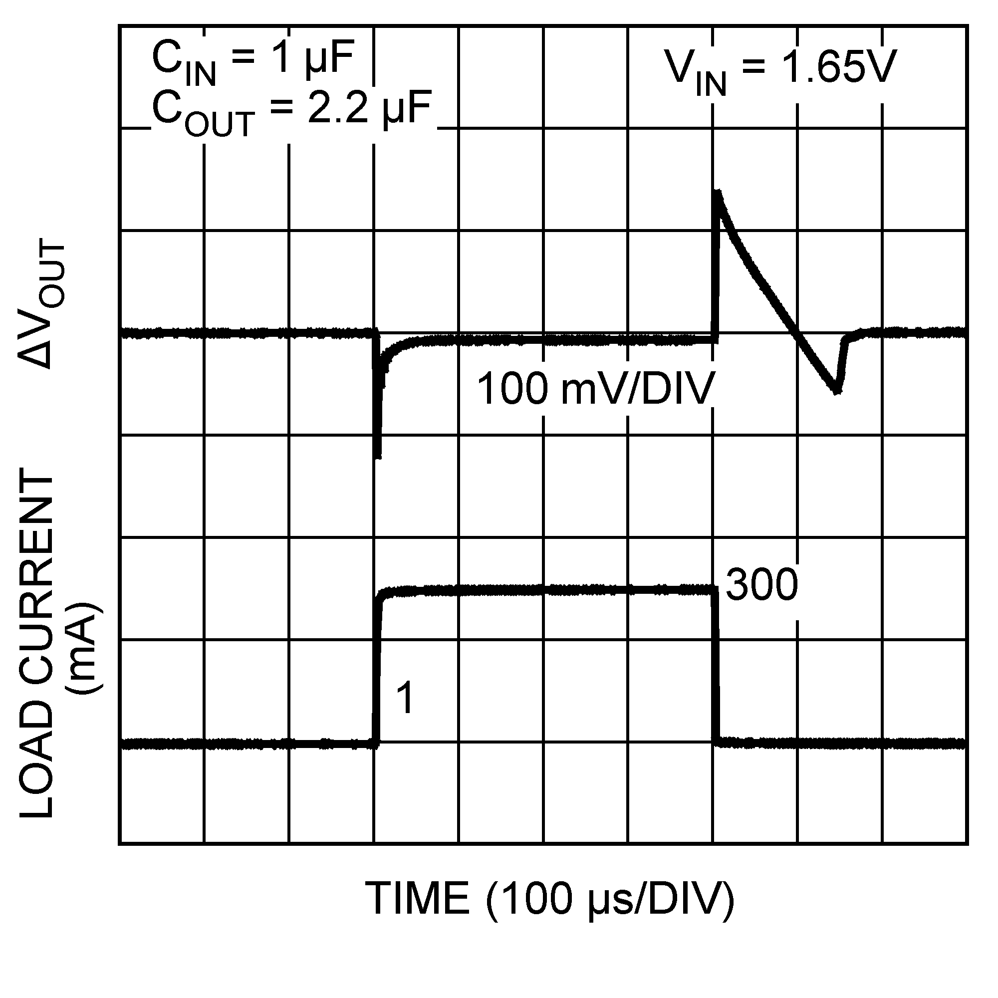
| VOUT = 1.5 V |
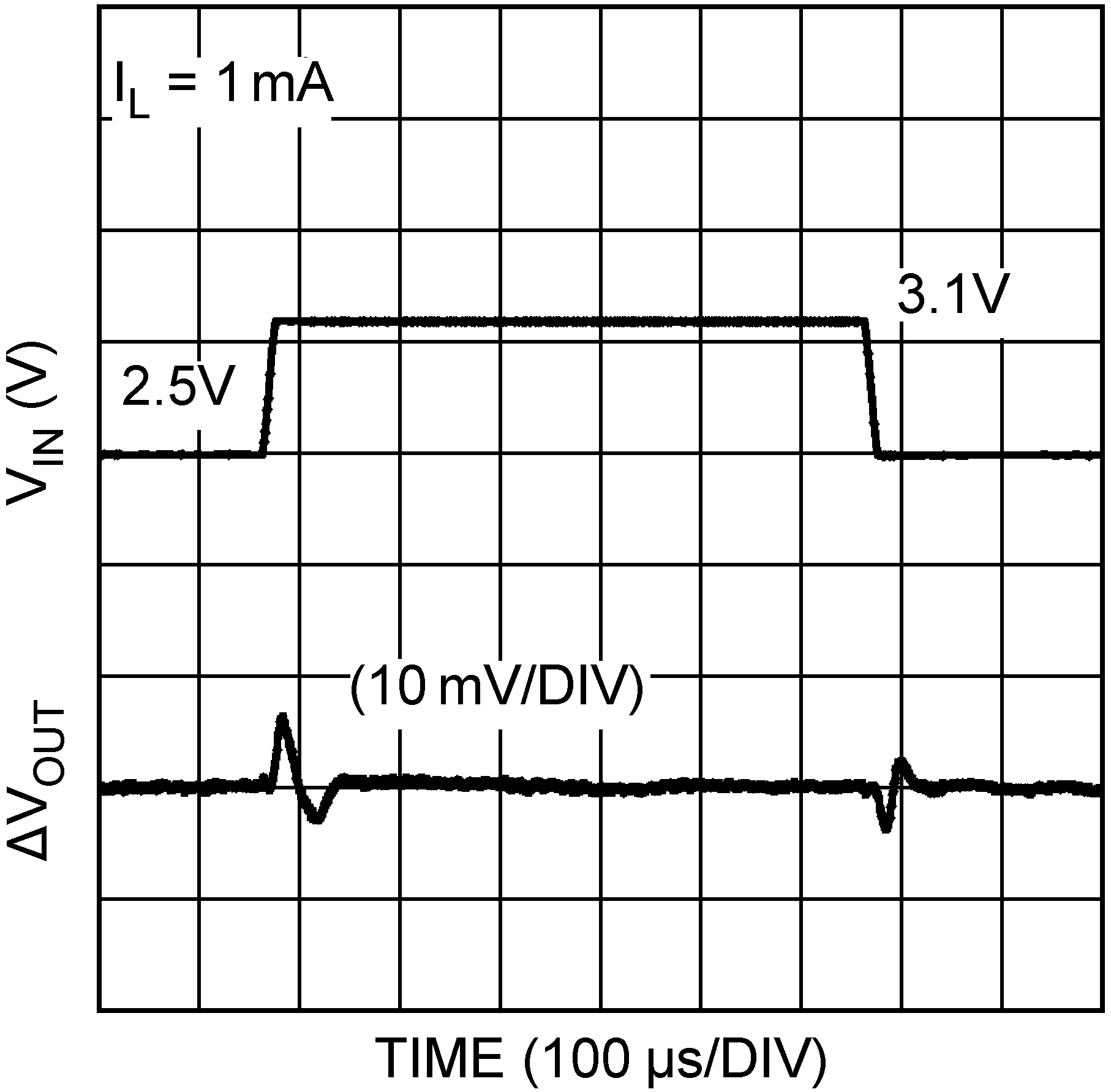
| ILOAD = 1 mA |
| VOUT = 1.2 V |
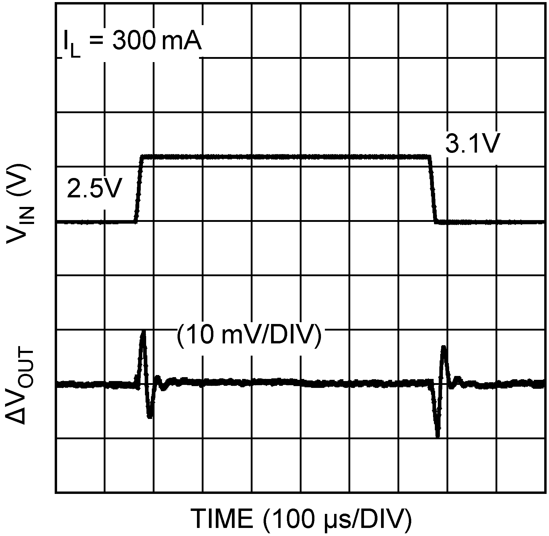
| ILOAD = 300 mA |