-
LP50xx 18-, 24-Channel, 12-Bit, PWM Ultralow-Quiescent-Current, I2C RGB LED Drivers
- 1
- 1 Features
- 2 Applications
- 3 Description
- 4 Description (continued)
- 5 Pin Configuration and Functions
- 6 Specifications
-
7 Detailed Description
- 7.1 Overview
- 7.2 Functional Block Diagram
- 7.3
Feature Description
- 7.3.1 PWM Control for Each Channel
- 7.3.2 LED Bank Control
- 7.3.3 Current Range Setting
- 7.3.4 Automatic Power-Save Mode
- 7.3.5 Protection Features
- 7.4 Device Functional Modes
- 7.5 Programming
- 7.6
Register Maps
- 7.6.1 DEVICE_CONFIG0 (Address = 0h) [reset = 0h]
- 7.6.2 DEVICE_CONFIG1 (Address = 1h) [reset = 3Ch]
- 7.6.3 LED_CONFIG0 (Address = 2h) [reset = 00h]
- 7.6.4 BANK_BRIGHTNESS (Address = 3h) [reset = FFh]
- 7.6.5 BANK_A_COLOR (Address = 4h) [reset = 00h]
- 7.6.6 BANK_B_COLOR (Address = 5h) [reset = 00h]
- 7.6.7 BANK_C_COLOR (Address = 6h) [reset = 00h]
- 7.6.8 LED0_BRIGHTNESS (Address = 7h) [reset = FFh]
- 7.6.9 LED1_BRIGHTNESS (Address = 8h) [reset = FFh]
- 7.6.10 LED2_BRIGHTNESS (Address = 9h) [reset = FFh]
- 7.6.11 LED3_BRIGHTNESS (Address = 0Ah) [reset = FFh]
- 7.6.12 LED4_BRIGHTNESS (Address = 0Bh) [reset = FFh]
- 7.6.13 LED5_BRIGHTNESS (Address = 0Ch) [reset = FFh]
- 7.6.14 LED6_BRIGHTNESS (Address = 0Dh) [reset = FFh]
- 7.6.15 LED7_BRIGHTNESS (Address = 0Eh) [reset = FFh]
- 7.6.16 OUT0_COLOR (Address = 0Fh) [reset = 00h]
- 7.6.17 OUT1_COLOR (Address = 10h) [reset = 00h]
- 7.6.18 OUT2_COLOR (Address = 11h) [reset = 00h]
- 7.6.19 OUT3_COLOR (Address = 12h) [reset = 00h]
- 7.6.20 OUT4_COLOR (Address = 13h) [reset = 00h]
- 7.6.21 OUT5_COLOR (Address = 14h) [reset = 00h]
- 7.6.22 OUT6_COLOR (Address = 15h) [reset = 00h]
- 7.6.23 OUT7_COLOR (Address = 16h) [reset = 00h]
- 7.6.24 OUT8_COLOR (Address = 17h) [reset = 00h]
- 7.6.25 OUT9_COLOR (Address = 18h) [reset = 00h]
- 7.6.26 OUT10_COLOR (Address = 19h) [reset = 00h]
- 7.6.27 OUT11_COLOR (Address = 1Ah) [reset = 00h]
- 7.6.28 OUT12_COLOR (Address = 1Bh) [reset = 00h]
- 7.6.29 OUT13_COLOR (Address = 1Ch) [reset = 00h]
- 7.6.30 OUT14_COLOR (Address = 1Dh) [reset = 00h]
- 7.6.31 OUT15_COLOR (Address = 1Eh) [reset = 00h]
- 7.6.32 OUT16_COLOR (Address = 1Fh) [reset = 00h]
- 7.6.33 OUT17_COLOR (Address = 20h) [reset = 00h]
- 7.6.34 OUT18_COLOR (Address = 21h) [reset = 00h]
- 7.6.35 OUT19_COLOR (Address = 22h) [reset = 00h]
- 7.6.36 OUT20_COLOR (Address = 23h) [reset = 00h]
- 7.6.37 OUT21_COLOR (Address = 24h) [reset = 00h]
- 7.6.38 OUT22_COLOR (Address = 25h) [reset = 00h]
- 7.6.39 OUT23_COLOR (Address = 26h) [reset = 00h]
- 7.6.40 RESET (Address = 27h) [reset = 00h]
- 8 Application and Implementation
- 9 Device and Documentation Support
- 10Revision History
- 11Mechanical, Packaging, and Orderable Information
- IMPORTANT NOTICE
Package Options
Mechanical Data (Package|Pins)
- RSM|32
Thermal pad, mechanical data (Package|Pins)
- RSM|32
Orderable Information
LP50xx 18-, 24-Channel, 12-Bit, PWM Ultralow-Quiescent-Current, I2C RGB LED Drivers
1 Features
- Operating voltage range:
- VCC range: 2.7V to 5.5V
- EN, SDA, and SCL pins compatible with
1.8V, 3.3V, and 5V power rails - Output maximum voltage: 6V
- 24 constant-current sinks with high precision
- 25.5mA maximum per channel with VCC in full range
- 35mA maximum per channel when VCC ≥ 3.3V
- Device-to-device error: ±7%; channel-to-channel error: ±7%
- Ultralow quiescent current:
- Shutdown mode: 1µA (maximum) with EN low
- Power saving mode: 10µA (typical) with EN high and all LEDs off for > 30ms
- Integrated 12-bit, 29kHz PWM generator for each channel:
- Independent color-mixing register per channel
- Independent brightness-control register per RGB LED module
- Optional logarithmic- or linear-scale brightness control
- Integrated 3-phase PWM-shifting scheme
- 3 programmable banks (R, G, B) for easy software control of each color
- 2 external hardware address pins allow connecting up to 4 devices
- Broadcast slave address allows configuring multiple devices simultaneously
- Auto-increment allows writing or reading consecutive registers within one transmission
- Up to 400kHz fast-mode I2C speed
2 Applications
LED lighting, indicator lights, and fun lights for:
- Smart speaker (with voice assistant)
- Smart home appliances
- Video doorbell
- Electronic smart lock
- Smoke and heat detector
- STB and DVR
- Smart router
- Handheld device
3 Description
In smart homes and other applications that use human-machine-interaction, high-performance RGB LED drivers are required. LED animation effects such as flashing, breathing, and chasing greatly improve user experience, and minimal system noise is essential.
The LP50xx device is an 18- or 24-channel constant current sink LED driver. The LP50xx device includes integrated color mixing and brightness control, and pre-configuration simplifies the software coding process. Integrated 12-bit, 29kHz PWM generators for each channel enable smooth, vivid color for LEDs, and eliminate audible noise.
| PART NUMBER | PACKAGE | BODY SIZE (NOM) |
|---|---|---|
| LP5024 | VQFN (32) | 4.00mm × 4.00mm |
| LP5018 | VQFN (32) | 4.00mm × 4.00mm |
| VSSOP (28) | 7.30mm × 3.00mm |
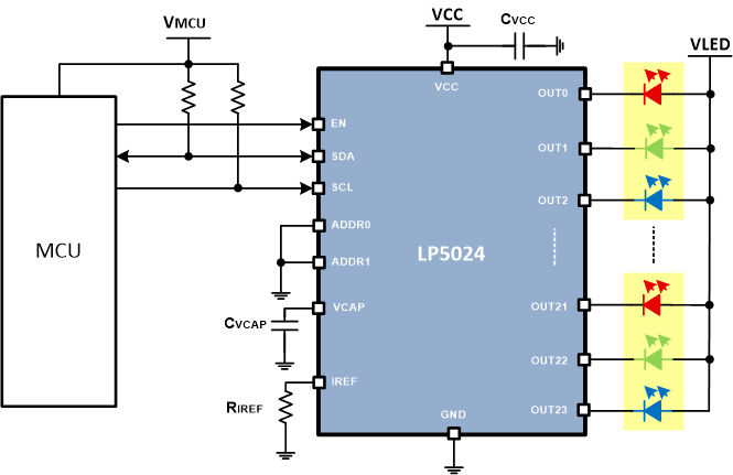
 Simplified Schematic