SNVS440B May 2007 – March 2016 LP5520
PRODUCTION DATA.
- 1 Features
- 2 Applications
- 3 Description
- 4 Revision History
- 5 Pin Configuration and Function
-
6 Specifications
- 6.1 Absolute Maximum Ratings
- 6.2 ESD Ratings
- 6.3 Recommended Operating Conditions
- 6.4 Thermal Information
- 6.5 Electrical Characteristics
- 6.6 RGB Driver Electrical Characteristics (ROUT, GOUT, BOUT Outputs)
- 6.7 Logic Interface Characteristics
- 6.8 Magnetic Boost DC-DC Converter Electrical Characteristics
- 6.9 I2C Timing Parameters
- 6.10 SPI Timing Requirements
- 6.11 Typical Characteristics
- 7 Detailed Description
- 8 Application and Implementation
- 9 Power Supply Recommendations
- 10Layout
- 11Device and Documentation Support
- 12Mechanical, Packaging, and Orderable Information
Package Options
Mechanical Data (Package|Pins)
- YZR|25
Thermal pad, mechanical data (Package|Pins)
Orderable Information
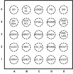
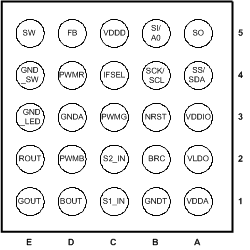
5 Pin Configuration and Function
YZR Packge
25-Pin DSBGA
Top View

YZR Packge
25-Pin DSBGA
Bottom View

Pin Functions
| PIN | TYPE | DESCRIPTION | |
|---|---|---|---|
| NUMBER | NAME | ||
| 1A | VDDA | Power | Supply voltage for analog circuitry |
| 1B | GNDT | Ground | Ground/Test |
| 1C | S1_IN | Input | ADC input 1, input for temperature sensor |
| 1D | BOUT | Output | Blue LED output |
| 1E | GOUT | Output | Green LED output |
| 2A | VLDO | Power | Internal LDO output |
| 2B | BRC | Logic Input | Brightness control for all LED outputs |
| 2C | S2_IN | Input | ADC input 2, input for optional second sensor |
| 2D | PWMB | Logic Input | PWM control for output B |
| 2E | ROUT | Output | Red LED output |
| 3A | VDDIO | Power | Supply voltage for input/output buffers and drivers |
| 3B | NRST | Logic Input | Master reset, active low |
| 3C | PWMG | Logic Input | PWM control for output G |
| 3D | GNDA | Ground | Ground for analog circuitry |
| 3E | GND_LED | Ground | Ground for LED currents |
| 4A | SS/SDA | Logic Input/Output | Slave select (SPI), serial data in/out (I2C) |
| 4B | SCK/SCL | Logic Input | Clock (SPI/I2C) |
| 4C | IFSEL | Logic Input | Interface selection (SPI or I2C-compatible, IF_SEL = 1 for SPI) |
| 4D | PWMR | Logic Input | PWM control for output R |
| 4E | GND_SW | Ground | Power switch ground |
| 5A | SO | Logic Output | Serial data out (SPI) |
| 5B | SI/A0 | Logic Input | Serial input (SPI), address select (I2C) |
| 5C | VDDD | Power | Supply voltage for digital circuitry |
| 5D | FB | Input | Boost converter feedback |
| 5E | SW | Output | Boost converter power switch |