SNVS820B APRIL 2013 – December 2016 LP5562
PRODUCTION DATA.
- 1 Features
- 2 Applications
- 3 Description
- 4 Revision History
- 5 Pin Configuration and Functions
-
6 Specifications
- 6.1 Absolute Maximum Ratings
- 6.2 ESD Ratings
- 6.3 Recommended Operating Conditions
- 6.4 Thermal Information
- 6.5 Electrical Characteristics
- 6.6 Logic Interface Characteristics
- 6.7 Recommended External Clock Source Conditions
- 6.8 I2C Timing Requirements (SDA, SCL)
- 6.9 Typical Characteristics: Current Consumption
- 6.10 Typical Characteristics: LED Output
-
7 Detailed Description
- 7.1 Overview
- 7.2 Functional Block Diagram
- 7.3
Feature Description
- 7.3.1 LED Drivers Operational Description
- 7.3.2 Direct I2C Register PWM Control Example
- 7.3.3 Program Execution Engines
- 7.3.4 Power-Save Mode
- 7.3.5 External Clock
- 7.3.6 Thermal Shutdown
- 7.3.7 Logic Interface Operational Description
- 7.3.8 I/O Levels
- 7.3.9 ADDR_SEL0, ADDR_SEL1 Pins
- 7.3.10 CLK_32 Pin
- 7.4 Device Functional Modes
- 7.5 Programming
- 7.6
Register Maps
- 7.6.1 Enable Register (Enable) (Address = 00h) [reset = 00h]
- 7.6.2 Operation Mode Register (OP Mode) (address = 01h) [reset = 00h]
- 7.6.3 B LED Output PWM Control Register (B_PWM) (address = 02h) [reset = 00h]
- 7.6.4 G LED Output PWM Control Register (G_PWM) (address = 03h) [reset = 00h]
- 7.6.5 R LED Output PWM Control Register (R_PWM) (address = 04h) [reset = 00h]
- 7.6.6 B LED Output Current Control Register (B_CURRENT)(address = 05h) [reset = AFh]
- 7.6.7 G LED Output Current Control Register (G_CURRENT)(address = 06h) [reset = AFh]
- 7.6.8 R LED Output Current Control Register (R_CURRENT) (address = 07h) [reset = AFh]
- 7.6.9 Configuration Control Register (CONFIG) (address = 08h) [reset = 00h]
- 7.6.10 Engine 1 Program Counter Value Register (Engine 1 PC) (address = 09h) [reset = 00h]
- 7.6.11 Engine 2 Program Counter Value Register (Engine 2 PC) (address = 0Ah) [reset = 00h]
- 7.6.12 Engine 3 Program Counter Value Register (Engine 3 PC) (address = 0Ah) [reset = 00h]
- 7.6.13 STATUS/INTERRUPT Register (address = 0Ch) [reset = 00h]
- 7.6.14 RESET Register (address = 0Dh) [reset = 00h]
- 7.6.15 WLED Output PWM Control Register (W_PWM) (address = 0Eh) [reset = 00h]
- 7.6.16 W LED Output Current Control Register (W_CURRENT) (address = 0Fh) [reset = AFh]
- 7.6.17 LED Mapping Register (LED Map) (address = 70h) [reset = 39h]
- 7.6.18 Program Memory (address = 10h - 6Fh) [reset = 00h]
- 8 Application and Implementation
- 9 Power Supply Recommendation
- 10Layout
- 11Device and Documentation Support
- 12Mechanical, Packaging, and Orderable Information
Package Options
Mechanical Data (Package|Pins)
- YQE|12
Thermal pad, mechanical data (Package|Pins)
Orderable Information
7 Detailed Description
7.1 Overview
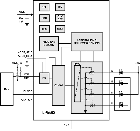
The LP5562 is a RGBW LED driver for indicator LED and keypad lighting. The device has an internal program memory for creating a variety of lighting sequences. When the program memory has been loaded, the LP5562 can operate independently without processor control.
The device has 4 LED drivers that are constant current sinks with 8-bit current and 8-bit PWM control. The current sinks can be controlled via the three execution engines or direct PWM control. The execution engines have five different functions used to build lighting sequences: Ramp, Set PWM, Go to Start, Branch, or End Trigger. These control methods and functions are explained in detail in Feature Description and Device Functional Modes.
7.2 Functional Block Diagram
7.3 Feature Description
7.3.1 LED Drivers Operational Description
The LP5562 has 4 LED drivers that are constant current sinks with 8-bit current and 8-bit PWM control. Current is controlled from I2C registers. PWM can be controlled with program execution engines or direct I2C register writes.
7.3.1.1 LED Driver Current Control
LED driver output current can be programmed with I2C register from 0 mA up to 25.5 mA. Current setting resolution is 100 μA (8-bit control).
Table 1. B_CURRENT Register (05h), G_CURRENT Register (06h), R_CURRENT Register (07h), W CURRENT Register (0Fh)
| NAME | BIT | DESCRIPTION | |||
|---|---|---|---|---|---|
| CURRENT | 7:0 | CURRENT SETTING | |||
| bin | hex | dec | mA | ||
| 0000 0000 | 00 | 0 | 0.0 | ||
| 0000 0001 | 01 | 1 | 0.1 | ||
| 0000 0010 | 02 | 2 | 0.2 | ||
| 0000 0011 | 03 | 3 | 0.3 | ||
| 0000 0100 | 04 | 4 | 0.4 | ||
| 0000 0101 | 05 | 5 | 0.5 | ||
| 0000 0110 | 06 | 6 | 0.6 | ||
| ... | ... | ... | ... | ||
| 1010 1111 | AF | 175 | 17.5 (def) | ||
| ... | ... | ... | ... | ||
| 1111 1011 | FB | 251 | 25.1 | ||
| 1111 1100 | FC | 252 | 25.2 | ||
| 1111 1101 | FS | 253 | 25.3 | ||
| 1111 1110 | FE | 254 | 25.4 | ||
| 1111 1111 | FF | 255 | 25.5 | ||
7.3.1.2 Controlling LED Driver Output PWM
PWM can be controlled by either with program execution engines (1, 2 and 3) or via I2C registers (02h for B, 03h for G, 04h for R and 0Eh for W).
Control of LED driver output PWM selection is managed with 2 bits for each LED output from register 70h. The Table 3 describes the selection options. With these bits for example all LED outputs can be controlled from one program execution engine.
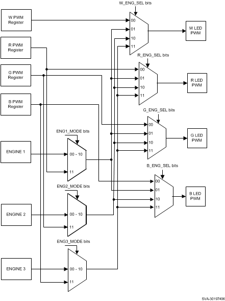 Figure 14. Controlling LED Outputs
The LED driver PWM control with 8-bit I2C register is defined in Table 2.
Table 2. LED Driver PWM Control Bits Register 70h
| NAME | BIT | DESCRIPTION |
|---|---|---|
| PWM | 7:0 | LED PWM value during I2C control operation mode |
| 0000 0000 = 0% PWM | ||
| 1111 1111 = 100% PWM |
If the LED driver outputs are controlled with engines, the engine adjusts the PWM according to the program code. However, when the engine mode bits are set to ‘11’, the engine is set to direct mode. In direct mode the PWM controls of engines comes:
- Engine 1 PWM control comes from B PWM I2C register (02h)
- Engine 2 PWM control comes from G PWM I2C register (03h)
- Engine 3 PWM control comes from R PWM I2C register (04h)
When the engine mode bits are set to '11' along with the LED PWM Output selection bits, it is possible to control all LED outputs from one I2C register.
Table 3. LED PWM Output Selection Bits
| B_ENG_SEL bits[1:0] G_ENG_SEL bits[3:2] R_ENG_SEL bits[5:4] W_ENG_SEL bits[7:6] |
DESCRIPTION |
|---|---|
| 00 | Output is controlled via I2C registers |
| 01 | ENG1_MODE and ENG1_EXEC register control LED output PWM instead of I2C register |
| 10 | ENG2_MODE and ENG2_EXEC register control LED output PWM instead of I2C register |
| 11 | ENG3_MODE and ENG3_EXEC register control LED output PWM instead of I2C register |
7.3.2 Direct I2C Register PWM Control Example
- Device Start-up
- Supply 3.6 V to VDD
- Supply 1.8 V to EN
- Wait 1 ms
- Write to address 00h 0100 0000b (chip_en to '1')
- Wait 500 μs (start-up delay)
- Use internal clock
- Write to address 08h 0000 0001b (enable internal clock)
- Direct PWM control
- Write to address 70h 0000 0000b (Configure all LED outputs to be controlled from I2C registers)
- Write PWM values
- Write to address 02h 1000 0000b (B driver PWM 50% duty cycle)
- Write to address 03h 1100 0000b (G driver PWM 75% duty cycle)
- Write to address 04h 1111 1111b (R driver PWM 100% duty cycle)
LEDs are turned on after the PWM values are written. Changes to the PWM value registers are reflected immediately to the LED brightness. Default LED current (17.5 mA) is used for LED outputs, if no other values are written.
PWM frequency is either 256 Hz or 558 Hz. Frequency is set with PWM_HF bit in register 08h. When PWM_HF is 0, the frequency is 256 Hz. When the PWM_HF bit is 1, the PWM frequency is 558 Hz. Brightness adjustment is either linear or logarithmic. This can be set with LOG_EN bit in register 00h. When LOG_EN = 0 linear adjustment scale is used and when LOG_EN = 1 logarithmic scale is used. By using logarithmic scale the visual effect seems linear to the eye. Register control bits are presented in following tables:
Table 4. ENABLE Register (00h)
| NAME | BIT | DESCRIPTION |
|---|---|---|
| LOG_EN | 7 | Logarithmic PWM adjustment enable bit |
| 0 = Linear adjustment | ||
| 1 = Logarithmic adjustment |
Table 5. CONFIG Register (08h)
| NAME | BIT | DESCRIPTION |
|---|---|---|
| PWM_HF | 6 | PWM clock frequency |
| 0 = 256 Hz | ||
| 1 = 558 Hz |
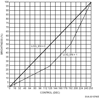 Figure 15. Logarithmic and Linear PWM Adjustment Curves
7.3.3 Program Execution Engines
Use of program execution engines is the other LED output PWM control method available in the LP5562. The device has 3 program execution engines. These engines create PWM controlled lighting patterns to the mapped LED outputs according to program codes developed by the user. Program coding is done using programming commands (see Program Execution Engine Programming Commands.) Programs are loaded into SRAM memory and engine control bits are used to run these programs autonomously. LED outputs can be mapped into these 3 engines with register 70h bit settings (see Table 3). The engines have different operation modes, program execution states, and program counters. Each engine has its own section of the SRAM memory.
7.3.3.1 Program Execution Engine States
Engine program execution is controlled from ENABLE register (00h). There are four different states for each engine, and these states are described in Table 6.
Table 6. ENABLE Register (00h)
| NAME | BIT | DESCRIPTION |
|---|---|---|
| ENG1_EXEC | 5:4 | Engine 1 program execution 00b = Hold: Wait until current command is finished then stop while EXEC mode is hold. PC can be read or written only in this mode. 01b = Step: Execute instruction defined by current Engine 1 PC value, increment PC, and change ENG1_EXEC to 00b (Hold). 10b = Run: Start at program counter value defined by current Engine 1 PC value. 11b = Execute instruction defined by current Engine 1 PC value and change ENG1_EXEC to 00b (Hold). |
| ENG2_EXEC | 3:2 | Engine 2 program execution 00b = Hold: Wait until current command is finished then stop while EXEC mode is hold. PC can be read or written only in this mode. 01b = Step: Execute instruction defined by current Engine 2 PC value, increment PC, and change ENG2_EXEC to 00b (Hold). 10b = Run: Start at program counter value defined by current Engine 2 PC value. 11b = Execute instruction defined by current Engine 2 PC value and change ENG2_EXEC to 00b (Hold). |
| ENG3_EXEC | 1:0 | Engine 3 program execution 00b = Hold: Wait until current command is finished then stop while EXEC mode is hold. PC can be read or written only in this mode. 01b = Step: Execute instruction defined by current engine 3 PC value, increment PC, and change ENG3_EXEC to 00b (Hold). 10b = Run: Start at program counter value defined by current engine 3 PC value. 11b = Execute instruction defined by current engine 3 PC value and change ENG3_EXEC to 00b (Hold). |
7.3.3.2 Program Execution Engine Operation Modes
Operation modes are defined in register address 01h. Each engine (1, 2, 3) operation mode can be configured separately. Mode registers are synchronized to a 32-kHz clock. Delay between consecutive I2C writes to OP_MODE register (01h) need to be longer than 153 μs (typ).
Table 7. Operation Mode Register (OP_MODE (01h))
| NAME | BIT | DESCRIPTION |
|---|---|---|
| ENG1_MODE | 5:4 | Engine 1 operation mode 00b = Disabled, reset engine 1 PC 01b = Load program to SRAM, reset engine 1 PC 10b = Run program defined by ENG1_EXEC 11b = Direct control from B PWM I2C register, reset engine 1 PC |
| ENG2_MODE | 3:2 | Engine 2 operation mode 00b = Disabled, reset engine 2 PC 01b = Load program to SRAM, reset engine 2 PC 10b = Run program defined by ENG2_EXEC 11b = Direct control from G PWM I2C register, reset engine 2 PC |
| ENG3_MODE | 1:0 | Engine 3 operation mode 00b = Disabled, reset engine 3 PC 01b = Load program to SRAM, reset engine 3 PC 10b = Run program defined by ENG3_EXEC 11b = Direct control from R PWM I2C register, reset engine 3 PC |
7.3.3.2.1 Operation Modes
-
Disabled
- Each channel can be configured to disabled mode. For the current engine mapped LED output brightness will be 0 during this mode. Disabled mode resets respective engine’s PC.
-
Load program
- LP5562 can store 16 commands for each engine (1, 2, 3). Each command consists of 16 bits. Because one register has only 8 bits, one command requires two I2C register addresses. In order to reduce program load time the LP5562 supports address auto increment. Register address is incremented after each 8 data bits. The whole program memory can be written in one I2C write sequence. Program memory is defined in the LP5562 register table, from address 10h to address 2Fh for engine 1, from address 30h to address 4Fh for engine 2, and from address 50h to address 6Fh for engine 3. In order to access program memory at least one channel operation mode needs to be load program.
- SRAM memory writes are allowed only to the channel in load program mode. All engines are in hold while one or several engines are in load program mode, and PWM values are frozen for the engines which are not in load programmode. Program execution continues when all engines are out of load program mode. Load program mode resets respective engine’s Program Counter (PC).
-
Run program
- Run program mode executes the commands defined in program memory for respective engine (1, 2, 3). Execution register bits in ENABLE register (00h) define how the program is executed. The program start position can be programmed to Program Counter register (see Table 8). By manually selecting the PC start value, user can write different lighting sequences to the SRAM memory, and select appropriate sequence with the PC register. If program counter runs to end (15), next command will be executed from program location 0. If internal clock is used in the run program mode, operation mode needs to be written disabled (00b) before disabling the chip (with CHIP_EN bit or EN pin) to ensure that the sequence starts from the correct program counter (PC) value when restarting the sequence. PC registers are synchronized to 32 kHz clock. Delay between consecutive I2C writes to Program Counter (PC) registers (09h, 0Ah, 0Bh) need to be longer than 153μs (typ.).
- Execution registers are synchronized to 32kHz clock. Delay between consecutive I2C writes to ENABLE register (00h) need to be longer than 488μs (typ.).
- Note that entering LOAD program or Direct Control Mode from RUN PROGRAM mode is not allowed. Engine execution mode should be set to Hold, and Operation Mode to disabled, when changing operation mode from RUN mode.
-
Direct control
- In Direct control mode the engine PWM output is controlled by R, G and B PWM I2C registers.
- When engine 1 is in Direct control mode, the engine 1 PWM output is controlled by B PWM I2C register (02h).
- When engine 2 is in Direct control mode, the engine 2 PWM output is controlled by G PWM I2C register (03h).
- When engine 3 is in Direct control mode, the engine 3 PWM output is controlled by R PWM I2C register (04h).
7.3.3.3 Program Execution Engine Program Counter (PC)
Program execution engine Program Counter tells the current program code command, which engine is executing. By setting the program counter value before starting the engine execution, user can set the starting point of the program execution.
Table 8. Engine1 PC Register (09h), Engine2 PC Register (0Ah), Engine3 PC Register (0Bh)
| NAME | BIT | DESCRIPTION |
|---|---|---|
| PC | 3:0 | Program counter value from 0 to 15d |
7.3.3.4 Program Execution Engine Programming Commands
The LP5562 has three independent programmable engines (1, 2, 3). Trigger connections between engines are common for all engines. All engines have own program memory sections for storing LED lighting patterns. Brightness control and patterns are done with 8-bit PWM control (256 steps) to get accurate and smooth color control. Program execution is timed with a 32.7-kHz clock. This clock can be generated internally or an external 32-kHz clock can be connected to the CLK_32K pin. Using an external clock enables synchronization of LED timing to this clock rather than an internal clock. Selection of the clock is made with address 08H bits INT_CLK_EN and CLK_DET_EN. See External Clock for details. Supported commands are listed in Table 9.
Table 9. LED Controller Programming Commands(1)
| Command | 15 | 14 | 13 | 12 | 11 | 10 | 9 | 8 | 7 | 6 | 5 | 4 | 3 | 2 | 1 | 0 |
|---|---|---|---|---|---|---|---|---|---|---|---|---|---|---|---|---|
| RampWait | 0 | Pre- scale | Step time | Sign | Increment (number of steps) | |||||||||||
| Set PWM | 0 | 1 | 0 | PWM Value | ||||||||||||
| Go to Start | 0 | 0 | 0 | 0 | 0 | 0 | 0 | 0 | 0 | 0 | 0 | |||||
| Branch | 1 | 0 | 1 | Loop count | x | Step / command number | ||||||||||
| End | 1 | 1 | 0 | Int | Reset | X | ||||||||||
| Trigger | 1 | 1 | 1 | X | X | X | Wait for trigger on engines 1, 2, 3 | X | X | X | Send trigger to engines 1,2, 3 | X | ||||
7.3.3.4.1 Ramp/Wait
The ramp command generates a PWM ramp starting from current value. At each ramp step the output is incremented by one. Time for one step is defined with Prescale and Step time bits. Minimum time for one step is 0.49 ms and maximum time is 63 × 15.6 ms = 1 second/step, so it is possible to program very fast and also very slow ramps. Increment value defines how many steps are taken in one command. Number of actual steps is Increment + 1. Maximum value is 127d, which corresponds to half of full-scale (128 steps). If during ramp command PWM reaches minimum/maximum (0/255) ramp command will be executed to the end and PWM will stay at minimum/maximum. This enables the ramp command to be used as combined ramp and wait command in a single instruction.
The ramp command can be used as wait instruction when increment is zero.
Setting register 00h bit LOG_EN sets the scale as either linear to logarithmic. When LOG_EN = 0, linear scale is used, and when LOG_EN = 1, logarithmic scale is used. By using logarithmic scale the visual effect of the ramp command seems linear to the eye.
Table 10. Ramp/Wait Command
| Ramp/Wait command | |||||||||||||||
|---|---|---|---|---|---|---|---|---|---|---|---|---|---|---|---|
| 15 | 14 | 13 | 12 | 11 | 10 | 9 | 8 | 7 | 6 | 5 | 4 | 3 | 2 | 1 | 0 |
| 0 | Pre- scale | Step time | Sign | Increment | |||||||||||
Table 11. Ramp/Wait Command Bits
| NAME | VALUE(d) | DESCRIPTION |
|---|---|---|
| Prescale | 0 | Divides master clock (32.768 Hz) by 16 = 2048 Hz, 0.49 ms cycle time |
| 1 | Divides master clock (32.768 Hz) by 512 = 64 Hz, 15.6 ms cycle time | |
| Step time | 1-63 | One ramp increment done in (step time) x (clock after prescale) Note: 0 means set PMW command. |
| Sign | 0 | Increase PWM output |
| 1 | Decrease PWM output | |
| Increment | 0-127 | The number of steps is Increment + 1. Note: 0 is a wait instruction. |
For example, if following parameters are used for ramp:
- Prescale = 1 ≥ cycle time = 15.6 ms
- Step time = 2 ≥ time = 15.6 ms × 2 = 31.2 ms
- Sign = 0 ≥ rising ramp Increment = 4 ≥ 5 cycles
Ramp command will be: 0100 0010 0000 0100b = 4204h
If current PWM value is 3, and the first command is as described above, the next command is a ramp with otherwise same the parameters, but with Sign = 1 (Command = 4284h), the result will be like in the following figure:
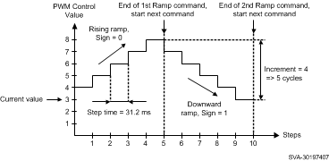 Figure 16. Example of 2 Sequential Ramp Commands
7.3.3.4.2 Set PWM
Set PWM output value from 0 to 255. Command takes sixteen 32-kHz clock cycles (= 488 μs). Setting register 00h bit LOG_EN sets the scale from linear to logarithmic.
Table 12. Set PWM Command Bits
| Set PWM command | |||||||||||||||
|---|---|---|---|---|---|---|---|---|---|---|---|---|---|---|---|
| 15 | 14 | 13 | 12 | 11 | 10 | 9 | 8 | 7 | 6 | 5 | 4 | 3 | 2 | 1 | 0 |
| 0 | 1 | 0 | 0 | 0 | 0 | 0 | 0 | PWM value | |||||||
7.3.3.4.3 Go-to-Start
Go-to-start command resets the Program Counter register and continues executing program from the 00h location. Command takes sixteen 32-kHz clock cycles. Note that default value for all program memory registers is 0000h, which is Go-to-Start command.
Table 13. Go-to-Start Command Bits
| Go-to-Start command | |||||||||||||||
|---|---|---|---|---|---|---|---|---|---|---|---|---|---|---|---|
| 15 | 14 | 13 | 12 | 11 | 10 | 9 | 8 | 7 | 6 | 5 | 4 | 3 | 2 | 1 | 0 |
| 0 | 0 | 0 | 0 | 0 | 0 | 0 | 0 | 0 | 0 | 0 | 0 | 0 | 0 | 0 | 0 |
7.3.3.4.4 Branch
When branch command is executed, the 'step number' value is loaded to PC, and program execution continues from this location. Looping is done by the number defined in loop count parameter. Nested looping is supported (loop inside loop). The number of nested loops is not limited. Command takes sixteen 32-kHz clock cycles.
Table 14. Branch Command (1)
| Branch command | |||||||||||||||
|---|---|---|---|---|---|---|---|---|---|---|---|---|---|---|---|
| 15 | 14 | 13 | 12 | 11 | 10 | 9 | 8 | 7 | 6 | 5 | 4 | 3 | 2 | 1 | 0 |
| 1 | 0 | 1 | Loop count | X | X | X | Step number | ||||||||
Table 15. Branch Command Bits
| NAME | VALUE | DESCRIPTION |
|---|---|---|
| loop count | 0-63 | The number of loops to be done. 0 means infinite loop. |
| step number | 0-15 | The step number to be loaded to program counter. |
7.3.3.4.5 End
End program execution resets the program counter and sets the corresponding EXEC register to 00b (hold). Command takes sixteen 32 kHz clock cycles.
Table 16. End Command (1)
| End command | |||||||||||||||
|---|---|---|---|---|---|---|---|---|---|---|---|---|---|---|---|
| 15 | 14 | 13 | 12 | 11 | 10 | 9 | 8 | 7 | 6 | 5 | 4 | 3 | 2 | 1 | 0 |
| 1 | 1 | 0 | int | reset | X | X | X | X | X | X | X | X | X | X | X |
Table 17. End Command Bits
| NAME | VALUE | DESCRIPTION |
|---|---|---|
| int | 0 | No interrupt will be sent. |
| 1 | Send interrupt by setting corresponding status register bit high to notify that program has ended. Interrupt can only be cleared by reading interrupt status register 0Ch. | |
| reset | 0 | Keep the current PWM value. |
| 1 | Set PWM value to 0. |
7.3.3.4.6 Trigger
Wait or send triggers can be used to synchronize operation between different engines. The send-trigger command takes sixteen 32-kHz clock cycles; the wait-for-trigger command takes at least sixteen 32-kHz clock cycles. The receiving engine stores sent triggers. Received triggers are cleared by wait for trigger command if received triggers match to engines defined in the command. Engine waits until all defined triggers have been received.
Table 18. Trigger Command(1)
| 15 | 14 | 13 | 12 | 11 | 10 | 9 | 8 | 7 | 6 | 5 | 4 | 3 | 2 | 1 | 0 |
|---|---|---|---|---|---|---|---|---|---|---|---|---|---|---|---|
| 1 | 1 | 1 | X | X | X | wait trigger <2:0> | X | X | X | send trigger <2:0> | X | ||||
| ENG3 | ENG2 | ENG1 | ENG3 | ENG2 | ENG1 | ||||||||||
Table 19. Trigger Command Bits
| NAME | VALUE(d) | DESCRIPTION |
|---|---|---|
| wait trigger<2:0> | 0-7 | Wait for trigger for the engine(s) defined. Several triggers can be defined in the same command. Bit 0 is engine 1, bit 1 is engine2, bit 2 is engine 3. |
| send trigger<2:0> | 0-7 | Send trigger for the engine(s) defined. Several triggers can be defined in the same command. Bit 0 is engine 1, bit 1 is engine2, bit 2 is engine 3. |
7.3.3.5 Program Load and Execution Example
- Start up device and configure device to SRAM write mode
- Supply 3.6V to VDD
- Supply 1.8V to EN
- Wait 1 ms
- Generate 32 kHz clock to CLK_32K pin
- Write to address 00h 0100 0000b (enable device)
- Wait 500 μs (startup delay)
- Write to address 01h 0001 0000b (configure engine 1 into 'Load program to SRAM' mode)
- Program load to SRAM
- Write to address 10h 0000 0011b (1st ramp command 8MSB)
- Write to address 11h 0111 1111b (1st ramp command 8 LSB)
- Write to address 12h 0100 1101b (1st wait command 8 MSB)
- Write to address 13h 0000 0000b (1st wait command 8 LSB)
- Write to address 14h 0000 0011b (2nd ramp command 8 MSB)
- Write to address 15h 1111 1111b (2nd ramp command 8 LSB)
- Write to address 16h 0110 0000b (2nd wait command 8 MSB)
- Write to address 17h 0000 0000b (2nd wait command 8 LSB)
- Enable Power Save and use external 32 kHz clock
- Write to address 08h 0010 0000b (enable powersave, use external clock)
- Run program
- Write to address 01h 0010 0000b (Configure LED controller operation mode to "Run program" in engine 1)
- Write to address 00h 0110 0000b (Configure program execution mode from "Hold" to "Run" in engine 1)
The LP5562 will generate a 1100 ms long LED pattern which will be repeated infinitely. The LED pattern is illustrated in the figure below.
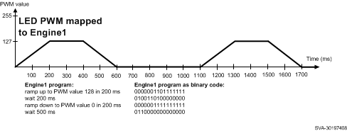 Figure 17. LED Lighting Pattern and Code for Program Load and Execution Example
7.3.4 Power-Save Mode
Automatic power save mode is enabled when the PS_EN bit in register address 08h is 1. Almost all analog blocks are powered down in power save, if an external clock is used. However, if an internal clock has been selected, only the LED drivers are disabled during power save since the digital part of the LED controller need to remain active. During program execution the LP5562 can enter power-save mode if there is no PWM activity in engine controlled outputs. To prevent short power-save sequences during program execution, the LP5562 has a command look-ahead filter. In each instruction cycle every engine commands are analyzed, and if there is sufficient time left with no PWM activity, the device will enter power save. In power save program execution continues uninterruptedly. When a command that requires PWM activity is executed, fast internal startup sequence will be started automatically. The following tables describe commands and conditions that can activate power save. All engines need to meet power-save conditions in order to enable power save.
Table 20. Engine Operation Mode and Power Save
| ENGINE OPERATION MODE | POWER SAVE CONDITION |
|---|---|
| 00b | Disabled mode enables power save |
| 01b | Load program to SRAM mode prevents power save. |
| 10b | Run program mode enables power save if there is no PWM activity and command look-ahead filter condition is met. |
| 11b | Direct control mode enables power save if there is no PWM activity. |
Table 21. Engine Commands and Power Save
| COMMAND | POWER SAVE CONDITION |
|---|---|
| Wait | No PWM activity and current command wait time longer than 50 ms. If prescale = 1 then wait time needs to be longer than 80 ms. |
| Ramp | Ramp command PWM value reaches minimum 0 and current command execution time left more than 50 ms. If prescale = 1 then time left needs to be more than 80 ms. |
| Trigger | No PWM activity during wait for trigger command execution. |
| End | No PWM activity or Reset bit = 1. |
| Set PWM | Enables power save if PWM set to 0 and next command generates at least 50 ms wait. |
| Other commands | No effect to power save. |
7.3.5 External Clock
The presence of an external clock can be detected by the LP5562. Program execution is clocked with an internal 32-kHz clock or with an external clock. Clocking is controlled with register address 08h bits, INT_CLK_EN, and CLK_DET_EN as seen in Table 22.
An external clock can be used if clock is present at the CLK_32K pin. The external clock frequency must be 32 kHz for the program execution PWM timing to be as specified. If higher or lower frequency is used, it will affect the program engine execution speed. If a clock frequency other than 32 kHz is used, the program execution timings must be scaled accordingly.
The LP5562 has automatic external clock detection. The external clock detector block only detects too low clock frequency (< 4 kHz), but it is recommended not to use external clock below 20 kHz. If external clock frequency is higher than specified, the external clock detector notifies that external clock is present. External clock status can be checked with read only bit EXT_CLK_USED in register address 0Ch, when the external clock detection is enabled (CLK_DET_EN bit = high). If EXT_CLK_USED = 1, then the external clock is detected and it is used for timing, if automatic clock selection is enabled.
If an external clock is stuck-at-zero or stuck-at-one, or the clock frequency is too low, the clock detector indicates that external clock is not present.
If an external clock is not used on the application, CLK_32K pin should be connected to GND to prevent floating of this pin and extra current consumption.
Table 22. CONFIG Register (08h)
| NAME | BIT | DESCRIPTION |
|---|---|---|
| CLK_DET_EN, INT_CLK_EN | 1:0 | LED Controller clock source |
| 00b = External clock source (CLK_32K) | ||
| 01b = Internal clock | ||
| 10b = Automatic selection | ||
| 11b = Internal clock |
7.3.6 Thermal Shutdown
If the LP5562 reaches thermal shutdown temperature (150°C typical) the device operation is disabled and the device state is in STARTUP mode, until no thermal shutdown event is present. Device will enter Normal mode when temperature drops below 130°C (typical) degrees.
Fault is cleared when thermal shutdown disappears.
7.3.7 Logic Interface Operational Description
The LP5562 features a flexible logic interface for connecting to processor and peripheral devices. Communication is done with the I2C-compatible interface, and different logic input/output pins makes it possible to synchronize operation of several devices.
7.3.8 I/O Levels
I2C interface, CLK_32K. ADDR_SEL0, and ADDR_SEL1 pins input levels are defined by voltage in EN pin. Using the EN pin as a voltage reference for logic inputs simplifies PCB routing and eliminates the need for a dedicated VIO pin. The following block diagram describes EN pin connections.
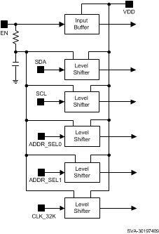 Figure 18. Using EN Pin as Digital I/O Voltage Reference
7.3.9 ADDR_SEL0, ADDR_SEL1 Pins
The ADDR_SEL0 and ADDR_SEL1 pins define the device I2C address. Pins are referenced to EN pin signal level. See I2C Addresses for I2C address definitions.
7.3.10 CLK_32 Pin
The CLK_32K pin is used for connecting an external 32-kHz clock to LP5562. An external clock can be used to synchronize the sequence engines of several LP5562 devices. Using an external clock can also improve automatic power save mode efficiency, because an internal clock can be switched off automatically when device has entered power-save mode, and an external clock is present. Device can be used without the external clock. If external clock is not used on the application, the CLK_32K pin should be connected to GND to prevent floating of this pin and extra current consumption.
7.4 Device Functional Modes
| RESET: | In the reset mode all the internal registers are reset to the default values. Reset is done always if FFh is written to Reset Register (0Dh) or internal Power On Reset is activated. Power On Reset (POR) will activate when supply voltage is connected or when the supply voltage VDD falls below 1.5 V (typical). Once VDD rises above 1.9 V (typical), POR will inactivate and the chip will continue to the standby mode. CHIP_EN control bit is low after POR by default. | |||
| STANDBY: | The standby mode is entered if the register bit CHIP_EN or EN pin is low and Reset is not active. This is the low power consumption mode, when all circuit functions are disabled. Registers can be written in this mode if EN pin is high. Control bits are effective after start up. | |||
| START-UP: | When CHIP_EN bit is written high and EN pin is high, the internal startup sequence powers up all the needed internal blocks (VREF, Bias, Oscillator etc.). Start-up delay after setting EN pin high is 1 ms (typical). Start-up delay after setting chip_en bit to '1' is 500 μs (typical). If the device temperature rises too high, the Thermal Shutdown (TSD) disables the device operation and the device state is in start-up mode, until no thermal shutdown event is present. | |||
| NORMAL: | During normal mode the user controls the device using the Control Registers. If EN pin is set low, the CHIP_EN bit is reset to 0. | |||
| POWER SAVE: | In power save mode analog blocks are disabled to minimize power consumption. See Power-Save Mode for further information. | |||
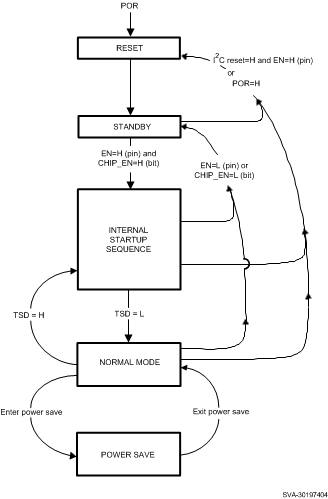 Figure 19. Modes of Operation
7.5 Programming
7.5.1 SRAM Memory
In the LP5562 there is a SRAM memory reserved for storing the LED lighting programs. Each engine has its own section of the memory so that engine 1 has registers 10h to 2Fh, engine 2 has registers 30h to 4Fh, and engine 3 has registers 50h to 6Fh. For each engine 16 engine commands (16-bit) can be stored. Each 16-bit command takes up two I2C registers.
Table 23. SRAM Memory Registers
| Address | Register | Bit7 | Bit6 | Bit5 | Bit4 | Bit3 | Bit2 | Bit1 | Bit0 |
|---|---|---|---|---|---|---|---|---|---|
| 10h | Prog mem ENG1 | COMMAND1_ENG1[15:8] | |||||||
| 11h | Prog mem ENG1 | COMMAND1_ENG1[7:0] | |||||||
| ... | |||||||||
| 2Eh | Prog mem ENG1 | COMMAND16_ENG1[15:8] | |||||||
| 2Fh | Prog mem ENG1 | COMMAND16_ENG1[7:0] | |||||||
| 30h | Prog mem ENG2 | COMMAND1_ENG2[15:8] | |||||||
| 31h | Prog mem ENG2 | COMMAND1_ENG2[7:0] | |||||||
| ... | |||||||||
| 4Eh | Prog mem ENG2 | COMMAND16_ENG2[15:8] | |||||||
| 4Fh | Prog mem ENG2 | COMMAND16_ENG2[7:0] | |||||||
| 50h | Prog mem ENG3 | COMMAND1_ENG3[15:8] | |||||||
| 51h | Prog mem ENG3 | COMMAND1_ENG3[7:0] | |||||||
| ... | |||||||||
| 6Eh | Prog mem ENG3 | COMMAND16_ENG3[15:8] | |||||||
| 6Fh | Prog mem ENG3 | COMMAND16_ENG3[7:0] | |||||||
When downloading a program to the SRAM engine modes need to be set to Load mode (see Table 6). While loading sequential I2C writing can be used (repeated start see Figure 24). However, please note that sequential read of the SRAM is not possible.
7.5.2 I2C-Compatible Serial Bus Interface
7.5.2.1 Interface Bus Overview
The I2C compatible synchronous serial interface provides access to the programmable functions and registers on the device. This protocol uses a two-wire interface for bidirectional communications between the IC's connected to the bus. The two interface lines are the Serial Data Line (SDA), and the Serial Clock Line (SCL). These lines should be connected to a positive supply, via a pullup resistor and remain HIGH even when the bus is idle.
Every device on the bus is assigned a unique address and acts as either a Master or a Slave depending on whether it generates or receives the serial clock (SCL).
7.5.2.2 Data Transactions
One data bit is transferred during each clock pulse. Data is sampled during the high state of the serial clock (SCL). Consequently, throughout the clock’s high period, the data should remain stable. Any changes on the SDA line during the high state of the SCL and in the middle of a transaction, aborts the current transaction. New data should be sent during the low SCL state. This protocol permits a single data line to transfer both command/control information and data using the synchronous serial clock.
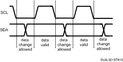 Figure 20. Data Validity
Each data transaction is composed of a Start Condition, a number of byte transfers (set by the software) and a Stop Condition to terminate the transaction. Every byte written to the SDA bus must be 8 bits long and is transferred with the most significant bit first. After each byte, an Acknowledge signal must follow. The following sections provide further details of this process.
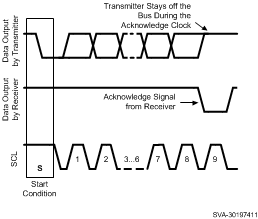 Figure 21. Acknowledge Signal
The Master device on the bus always generates the Start and Stop Conditions (control codes). After a Start Condition is generated, the bus is considered busy and it retains this status until a certain time after a Stop Condition is generated. A high-to-low transition of the data line (SDA) while the clock (SCL) is high indicates a Start Condition. A low-to-high transition of the SDA line while the SCL is high indicates a Stop Condition.
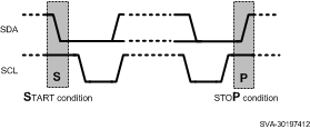 Figure 22. Start and Stop Conditions
In addition to the first Start Condition, a repeated Start Condition can be generated in the middle of a transaction. This allows another device to be accessed, or a register read cycle.
7.5.2.3 Acknowledge Cycle
The Acknowledge Cycle consists of two signals: the acknowledge clock pulse the master sends with each byte transferred, and the acknowledge signal sent by the receiving device.
The master generates the acknowledge clock pulse on the ninth clock pulse of the byte transfer. The transmitter releases the SDA line (permits it to go high) to allow the receiver to send the acknowledge signal. The receiver must pull down the SDA line during the acknowledge clock pulse and ensure that SDA remains low during the high period of the clock pulse, thus signaling the correct reception of the last data byte and its readiness to receive the next byte.
7.5.2.4 Acknowledge After Every Byte Rule
The master generates an acknowledge clock pulse after each byte transfer. The receiver sends an acknowledge signal after every byte received.
There is one exception to the “acknowledge after every byte” rule. When the master is the receiver, it must indicate to the transmitter an end of data by not-acknowledging (“negative acknowledge”) the last byte clocked out of the slave. This “negative acknowledge” still includes the acknowledge clock pulse (generated by the master), but the SDA line is not pulled down.
7.5.2.5 Addressing Transfer Formats
Each device on the bus has a unique slave address. The LP5562 operates as a slave device with the 7-bit address. LP5562 I2C address is pin selectable from four different choices. If 8-bit address is used for programming, the 8th bit is 1 for read and 0 for write. Table 24 shows the 8-bit I2C addresses.
Table 24. I2C Addresses
| ADDR_SEL [1:0] |
I 2 C ADDRESS WRITE (8 bits) |
I 2 C ADDRESS READ (8 bits) |
|---|---|---|
| 00 | 0110 0000 = 60h | 0110 0001 = 61h |
| 01 | 0110 0010 = 62h | 0110 0011 = 63h |
| 10 | 0110 0100 = 64h | 0110 0101 = 65h |
| 11 | 0110 0110 = 66h | 0110 0111 = 67h |
Before any data is transmitted, the master transmits the address of the slave being addressed.
The slave device should send an acknowledge signal on the SDA line, once it recognizes its address.
The slave address is the first seven bits after a Start Condition. The direction of the data transfer (R/W) depends on the bit sent after the slave address — the eighth bit.
When the slave address is sent, each device in the system compares this slave address with its own. If there is a match, the device considers itself addressed and sends an acknowledge signal. Depending upon the state of the R/W bit (1:read, 0:write), the device acts as a transmitter or a receiver.
 Figure 23. I2C chip address
7.5.2.6 Control Register Write Cycle
- Master device generates start condition.
- Master device sends slave address (7 bits) and the data direction bit (r/w = 0).
- Slave device sends acknowledge signal if the slave address is correct.
- Master sends control register address (8 bits).
- Slave sends acknowledge signal.
- Master sends data byte to be written to the addressed register.
- Slave sends acknowledge signal.
- If master will send further data bytes the control register address will be incremented by one after acknowledge signal.
- Write cycle ends when the master creates stop condition.
7.5.2.7 Control Register Read Cycle
- Master device generates a start condition.
- Master device sends slave address (7 bits) and the data direction bit (r/w = 0).
- Slave device sends acknowledge signal if the slave address is correct.
- Master sends control register address (8 bits).
- Slave sends acknowledge signal.
- Master device generates repeated start condition.
- Master sends the slave address (7 bits) and the data direction bit (r/w = 1).
- Slave sends acknowledge signal if the slave address is correct.
- Slave sends data byte from addressed register.
- If the master device sends acknowledge signal, the control register address will be incremented by one. Slave device sends data byte from addressed register.
- Read cycle ends when the master does not generate acknowledge signal after data byte and generates stop condition.
Table 25. I2C Data Read/Write Flow(1)
| ADDRESS MODE | |
|---|---|
| Data Read | <Start Condition> |
| <Slave Address><r/w = 0>[Ack] | |
| <Register Addr.>[Ack] | |
| <Repeated Start Condition> | |
| <Slave Address><r/w = 1>[Ack] | |
| [Register Data]<Ack or NAck> | |
| ... additional reads from subsequent register address possible | |
| <Stop Condition> | |
| Data Write | <Start Condition> |
| <Slave Address><r/w='0'>[Ack] | |
| <Register Addr.>[Ack] | |
| <Register Data>[Ack] | |
| ... additional writes to subsequent register address possible | |
| <Stop Condition> |
7.5.2.8 Register Read/Write Format
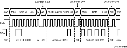 Figure 24. Register Write Format
When a read function is to be accomplished, a write function must precede the read function, as show in the Read Cycle waveform.
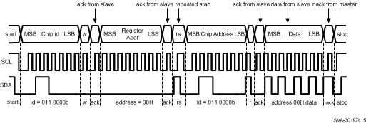 Figure 25. Register Read Format
w = write (SDA = 0)
r = read (SDA = 1)
ack = acknowledge (SDA pulled down by either master or slave)
rs = repeated start
id = 7-bit chip address
7.6 Register Maps
Table 26. LP5562 Control Register Names and Default Values
| ADDR (HEX) | REGISTER | D7 | D6 | D5 | D4 | D3 | D2 | D1 | D0 | DEFAULT |
|---|---|---|---|---|---|---|---|---|---|---|
| 00 | ENABLE | LOG_EN | CHIP_EN | ENG1_EXEC[1:0] | ENG2_EXEC[1:0] | ENG3_EXEC[1:0] | 0000 0000 | |||
| 01 | OP MODE | ENG1_MODE[1:0] | ENG2_MODE[1:0] | ENG3_MODE[1:0] | 0000 0000 | |||||
| 02 | B PWM | B_PWM[7:0] | 0000 0000 | |||||||
| 03 | G PWM | G_PWM[7:0] | 0000 0000 | |||||||
| 04 | R PWM | R_PWM[7:0] | 0000 0000 | |||||||
| 05 | B CURRENT | B_CURRENT[7:0] | 1010 1111 | |||||||
| 06 | G CURRENT | G_CURRENT[7:0] | 1010 1111 | |||||||
| 07 | R CURRENT | R_CURRENT[7:0] | 1010 1111 | |||||||
| 08 | CONFIG | PWM_HF | PS_EN | CLK_DET_EN | INT_CLK_E N | 0000 0000 | ||||
| 09 | ENG1 PC | ENG1_PC[3:0] | 0000 0000 | |||||||
| 0A | ENG2 PC | ENG2_PC[3:0] | 0000 0000 | |||||||
| 0B | ENG3 PC | ENG3_PC[3:0] | 0000 0000 | |||||||
| 0C | STATUS | EXT_CLK_USED | ENG1_INT | ENG2_INT | ENG3_INT | 0000 0000 | ||||
| 0D | RESET | RESET[7:0] | 0000 0000 | |||||||
| 0E | W PWM | W_PWM[7:0] | 00000000 | |||||||
| 0F | W CURRENT | W_CURRENT[7:0] | 10101111 | |||||||
| 70 | LED MAP | W_ENG_SEL | R_ENG_SEL | G_ENG_SEL | B_ENG_SEL | 00111001 | ||||
| 10 | PROG MEM ENG1 | CMD_1_ENG1[15:8] | 0000 0000 | |||||||
| 11 | PROG MEM ENG1 | CMD_1_ENG1[7:0] | 0000 0000 | |||||||
| ... | ||||||||||
| 2E | PROG MEM ENG1 | CMD_16_ENG1[15:8] | 0000 0000 | |||||||
| 2F | PROG MEM ENG1 | CMD_16_ENG1[7:0] | 0000 0000 | |||||||
| 30 | PROG MEM ENG2 | CMD_1_ENG2[15:8] | 0000 0000 | |||||||
| 31 | PROG MEM ENG2 | CMD_1_ENG2[7:0] | 0000 0000 | |||||||
| ... | ||||||||||
| 4E | PROG MEM ENG2 | CMD_16_ENG2[15:8] | 0000 0000 | |||||||
| 4F | PROG MEM ENG2 | CMD_16_ENG2[7:0] | 0000 0000 | |||||||
| 50 | PROG MEM ENG3 | CMD_1_ENG3[15:8] | 0000 0000 | |||||||
| 51 | PROG MEM ENG3 | CMD_1_ENG3[7:0] | 0000 0000 | |||||||
| ... | ||||||||||
| 6E | PROG MEM ENG3 | CMD_16_ENG3[15:8] | 0000 0000 | |||||||
| 6F | PROG MEM ENG3 | CMD_16_ENG3[7:0] | 0000 0000 | |||||||
7.6.1 Enable Register (Enable) (Address = 00h) [reset = 00h]
EXEC registers are synchronized to the 32-kHz clock. Delay between consecutive I2C writes to ENABLE register (00h) need to be longer than 488 μs (typical).
| 7 | 6 | 5 | 4 | 3 | 2 | 1 | 0 |
| LOG_EN | CHIP_EN | ENG1_EXEC[1:0] | ENG2_EXEC[1:0] | ENG3_EXEC[1:0] | |||
| R/W | R/W | R/W | R/W | R/W | |||
| LEGEND: R/W = Read/Write; R = Read only; -n = value after reset |
Table 27. Enable Register Field Descriptions
| Bit | Field | Type | Reset | Description |
|---|---|---|---|---|
| 7 | LOG_EN | R/W | Logarithmic PWM adjustment generation enable | |
| 6 | CHIP_EN | R/W | Master chip enable. Enables device internal startup sequence. See for further information. Setting EN pin low resets the CHIP_EN state to 0. Allow 500 µs delay after setting chip_en bit to '1' | |
| 5:4 | ENG1_EXEC | R/W | Engine 1 program execution. 00b = Hold: Wait until current command is finished then stop while EXEC mode is hold. PC can be read or written only in this mode. 01b = Step: Execute instruction defined by current engine 1 PC value, increment PC and change ENG1_EXEC to 00b (Hold) 10b = Run: Start at program counter value defined by current engine 1 PC value 11b = Execute instruction defined by current engine 1 PC value and change ENG1_EXEC to 00b (Hold) |
|
| 3:2 | ENG2_EXEC | R/W | Engine 2 program execution 00b = Hold: Wait until current command is finished then stop while EXEC mode is hold. PC can be read or written only in this mode. 01b = Step: Execute instruction defined by current engine 2 PC value, increment PC and change ENG2_EXEC to 00b (Hold) 10b = Run: Start at program counter value defined by current engine 2 PC value 11b = Execute instruction defined by current engine 2 PC value and change ENG2_EXEC to 00b (Hold) |
|
| ENG3_EXEC | 1:0 | R/W | Engine 3 program execution 00b = Hold: Wait until current command is finished then stop while EXEC mode is hold. PC can be read or written only in this mode. 01b = Step: Execute instruction defined by current engine 3 PC value, increment PC and change ENG3_EXEC to 00b (Hold) 10b = Run: Start at program counter value defined by current engine 3 PC value 11b = Execute instruction defined by current engine 3 PC value and change ENG3_EXEC to 00b (Hold) |
7.6.2 Operation Mode Register (OP Mode) (address = 01h) [reset = 00h]
MODE registers are synchronized to 32-kHz clock. Delay between consecutive I2C writes to OP_MODE register (01h) need to be longer than 153 μs (typ).
| 7 | 6 | 5 | 4 | 3 | 2 | 1 | 0 |
| ENG1_MODE[1:0] | ENG1_MODE[1:0] | ENG1_MODE[1:0] | |||||
| R/W | R/W | R/W | |||||
| LEGEND: R/W = Read/Write; R = Read only; -n = value after reset |
Table 28. OP Mode Register Field Descriptions
| Bit | Field | Type | Reset | Description |
|---|---|---|---|---|
| 5:4 | ENG1_MODE | R/W | Engine 1 operation mode 00b = Disabled 01b = Load program to SRAM, reset engine 1 PC 10b = Run program defined by ENG1_EXEC 11b = Direct control |
|
| 3:2 | ENG2_MODE | R/W | Engine 2 operation mode 00b = Disabled 01b = Load program to SRAM, reset engine 2 PC 10b = Run program defined by ENG2_EXEC 11b = Direct control |
|
| 1:0 | ENG3_MODE | R/W | Engine 3 operation mode 00b = Disabled 01b = Load program to SRAM, reset engine 3 PC 10b = Run program defined by ENG3_EXEC 11b = Direct control |
7.6.3 B LED Output PWM Control Register (B_PWM) (address = 02h) [reset = 00h]
| 7 | 6 | 5 | 4 | 3 | 2 | 1 | 0 |
| B_PWM[7:0] | |||||||
| R/W | |||||||
| LEGEND: R/W = Read/Write; R = Read only; -n = value after reset |
Table 29. B_PWM Register Field Descriptions
| Bit | Field | Type | Reset | Description |
|---|---|---|---|---|
| 7:0 | B_PWM | R/W | B LED output PWM value during direct control operation mode |
7.6.4 G LED Output PWM Control Register (G_PWM) (address = 03h) [reset = 00h]
| 7 | 6 | 5 | 4 | 3 | 2 | 1 | 0 |
| G_PWM[7:0] | |||||||
| R/W | |||||||
| LEGEND: R/W = Read/Write; R = Read only; -n = value after reset |
Table 30. G_PWM Register Field Descriptions
| Bit | Field | Type | Reset | Description |
|---|---|---|---|---|
| 7:0 | G_PWM | R/W | G LED output PWM value during direct control operation mode |
7.6.5 R LED Output PWM Control Register (R_PWM) (address = 04h) [reset = 00h]
| 7 | 6 | 5 | 4 | 3 | 2 | 1 | 0 |
| R_PWM[7:0] | |||||||
| R/W | |||||||
| LEGEND: R/W = Read/Write; R = Read only; -n = value after reset |
Table 31. R_PWM Register Field Descriptions
| Bit | Field | Type | Reset | Description |
|---|---|---|---|---|
| 7:0 | R_PWM | R/W | R LED output PWM value during direct control operation mode |
7.6.6 B LED Output Current Control Register (B_CURRENT)(address = 05h) [reset = AFh]
| 7 | 6 | 5 | 4 | 3 | 2 | 1 | 0 |
| B_CURRENT[7:0] | |||||||
| R/W | |||||||
| LEGEND: R/W = Read/Write; R = Read only; -n = value after reset |
Table 32. B_CURRENT Register Field Descriptions
| Bit | Field | Type | Reset | Description |
|---|---|---|---|---|
| 7:0 | B_CURRENT | R/W | Current setting 0000 0000b = 0.0 mA 0000 0001b = 0.1 mA 0000 0010b = 0.2 mA 0000 0011b = 0.3 mA 0000 0100b = 0.4 mA 0000 0101b = 0.5 mA 0000 0110b = 0.6 mA ... 1010 1111b = 17.5 mA (default) ... 1111 1011b = 25.1 mA 1111 1100b = 25.2 mA 1111 1101b = 25.3 mA 1111 1110b = 25.4 mA 1111 1111b = 25.5 mA |
7.6.7 G LED Output Current Control Register (G_CURRENT)(address = 06h) [reset = AFh]
| 7 | 6 | 5 | 4 | 3 | 2 | 1 | 0 |
| G_CURRENT[7:0] | |||||||
| R/W | |||||||
| LEGEND: R/W = Read/Write; R = Read only; -n = value after reset |
Table 33. G_CURRENT Register Field Descriptions
| Bit | Field | Type | Reset | Description |
|---|---|---|---|---|
| 7:0 | G_CURRENT | R/W | Current setting 0000 0000b = 0.0 mA 0000 0001b = 0.1 mA 0000 0010b = 0.2 mA 0000 0011b = 0.3 mA 0000 0100b = 0.4 mA 0000 0101b = 0.5 mA 0000 0110b = 0.6 mA ... 1010 1111b = 17.5 mA (default) ... 1111 1011b = 25.1 mA 1111 1100b = 25.2 mA 1111 1101b = 25.3 mA 1111 1110b = 25.4 mA 1111 1111b = 25.5 mA |
7.6.8 R LED Output Current Control Register (R_CURRENT) (address = 07h) [reset = AFh]
| 7 | 6 | 5 | 4 | 3 | 2 | 1 | 0 |
| R_CURRENT[7:0] | |||||||
| R/W | |||||||
| LEGEND: R/W = Read/Write; R = Read only; -n = value after reset |
Table 34. R_CURRENT Register Field Descriptions
| Bit | Field | Type | Reset | Description |
|---|---|---|---|---|
| 7:0 | R_CURRENT | R/W | Current setting 0000 0000b = 0.0 mA 0000 0001b = 0.1 mA 0000 0010b = 0.2 mA 0000 0011b = 0.3 mA 0000 0100b = 0.4 mA 0000 0101b = 0.5 mA 0000 0110b = 0.6 mA ... 1010 1111b = 17.5 mA (default) ... 1111 1011b = 25.1 mA 1111 1100b = 25.2 mA 1111 1101b = 25.3 mA 1111 1110b = 25.4 mA 1111 1111b = 25.5 mA |
7.6.9 Configuration Control Register (CONFIG) (address = 08h) [reset = 00h]
| 7 | 6 | 5 | 4 | 3 | 2 | 1 | 0 |
| PWM_HF | PS_EN | CLK_DET_EN | INT_CLK_EN | ||||
| R/W | R/W | R/W | R/W |
| LEGEND: R/W = Read/Write; R = Read only; -n = value after reset |
Table 35. CONFIG Register Field Descriptions
| Bit | Field | Type | Reset | Description |
|---|---|---|---|---|
| 6 | PWM_HF | R/W | PWM clock 0 = 256-Hz PWM clock used 1 = 558-Hz PWM clock used |
|
| 5 | PWRSAVE_EN | R/W | Power save mode enable | |
| 1:0 | CLK_DET_EN, INT_CLK_EN |
R/W | LED Controller clock source 00b = External clock source (CLK_32K) 01b = Internal clock 10b = Automatic selection 11b = Internal clock |
7.6.10 Engine 1 Program Counter Value Register (Engine 1 PC) (address = 09h) [reset = 00h]
PC registers are synchronized to a 32-kHz clock. Delay between consecutive I2C writes to PC registers needs to be longer than 153 μs (typical). PC register can be read or written only when EXEC mode is hold.
| 7 | 6 | 5 | 4 | 3 | 2 | 1 | 0 |
| ENG1_PC[3:0] | |||||||
| R/W | |||||||
| LEGEND: R/W = Read/Write; R = Read only; -n = value after reset |
Table 36. Engine 1 PC Register Field Descriptions
| Bit | Field | Type | Reset | Description |
|---|---|---|---|---|
| 3:0 | ENG1_PC | R/W | Engine 1 program counter value |
7.6.11 Engine 2 Program Counter Value Register (Engine 2 PC) (address = 0Ah) [reset = 00h]
PC registers are synchronized to 32-kHz clock. Delay between consecutive I2C writes to PC registers needs to be longer than 153 μs (typical). PC register can be read or written only when EXEC mode is hold.
| 7 | 6 | 5 | 4 | 3 | 2 | 1 | 0 |
| ENG2_PC[3:0] | |||||||
| R/W | |||||||
| LEGEND: R/W = Read/Write; R = Read only; -n = value after reset |
Table 37. Engine 2 PC Register Field Descriptions
| Bit | Field | Type | Reset | Description |
|---|---|---|---|---|
| 3:0 | ENG2_PC | R/W | Engine 2 program counter value |
7.6.12 Engine 3 Program Counter Value Register (Engine 3 PC) (address = 0Ah) [reset = 00h]
PC registers are synchronized to 32 kHz clock. Delay between consecutive I2C writes to PC registers needs to be longer than 153 μs (typ.). PC register can be read or written only when EXEC mode is hold.
| 7 | 6 | 5 | 4 | 3 | 2 | 1 | 0 |
| ENG3_PC[3:0] | |||||||
| R/W | |||||||
| LEGEND: R/W = Read/Write; R = Read only; -n = value after reset |
Table 38. Engine 3 PC Register Field Descriptions
| Bit | Field | Type | Reset | Description |
|---|---|---|---|---|
| 3:0 | ENG3_PC | R/W | Engine 3 program counter value |
7.6.13 STATUS/INTERRUPT Register (address = 0Ch) [reset = 00h]
Note:Register INT bits will be cleared when read operation to Status/Interrupt register occurs.
| 7 | 6 | 5 | 4 | 3 | 2 | 1 | 0 |
| EXT_CLK USED | ENG1_INT | ENG2_INT | ENG3_INT | ||||
| R | R | R | R |
| LEGEND: R/W = Read/Write; R = Read only; -n = value after reset |
Table 39. STATUS/INTERRUPT Register Field Descriptions
| Bit | Field | Type | Reset | Description |
|---|---|---|---|---|
| 3 | EXT_CLK USED | R | External clock state 0 = Internal clock used 1 = External 32kHz clock used |
|
| 2 | ENG1_INT | R | Interrupt from engine 1 | |
| 1 | ENG2_INT | R | Interrupt from engine 2 | |
| 0 | ENG3_INT | R | Interrupt from engine 3 |
7.6.14 RESET Register (address = 0Dh) [reset = 00h]
| 7 | 6 | 5 | 4 | 3 | 2 | 1 | 0 |
| RESET[7:0] | |||||||
| R/W | |||||||
| LEGEND: R/W = Read/Write; R = Read only; -n = value after reset |
Table 40. RESET Register Field Descriptions
| Bit | Field | Type | Reset | Description |
|---|---|---|---|---|
| 7:0 | RESET | R/W | Reset all register values when FFh is written. |
7.6.15 WLED Output PWM Control Register (W_PWM) (address = 0Eh) [reset = 00h]
| 7 | 6 | 5 | 4 | 3 | 2 | 1 | 0 |
| W_PWM[7:0] | |||||||
| R/W | |||||||
| LEGEND: R/W = Read/Write; R = Read only; -n = value after reset |
Table 41. W_PWM Register Field Descriptions
| Bit | Field | Type | Reset | Description |
|---|---|---|---|---|
| 7:0 | W_PWM | R/W | W LED Output PWM value during direct control operation mode |
7.6.16 W LED Output Current Control Register (W_CURRENT) (address = 0Fh) [reset = AFh]
| 7 | 6 | 5 | 4 | 3 | 2 | 1 | 0 |
| W_CURRENT[7:0] | |||||||
| R/W | |||||||
| LEGEND: R/W = Read/Write; R = Read only; -n = value after reset |
Table 42. W_CURRENT Register Field Descriptions
| Bit | Field | Type | Reset | Description |
|---|---|---|---|---|
| 7:0 | W_CURRENT | R/W | Current setting 0000 0000b = 0.0 mA 0000 0001b = 0.1 mA 0000 0010b = 0.2 mA 0000 0011b = 0.3 mA 0000 0100b = 0.4 mA 0000 0101b = 0.5 mA 0000 0110b = 0.6 mA ... 1010 1111b = 17.5 mA (default) ... 1111 1011b = 25.1 mA 1111 1100b = 25.2 mA 1111 1101b = 25.3 mA 1111 1110b = 25.4 mA 1111 1111b = 25.5 mA |
7.6.17 LED Mapping Register (LED Map) (address = 70h) [reset = 39h]
| 7 | 6 | 5 | 4 | 3 | 2 | 1 | 0 |
| W_ENG_SEL[1:0] | R_ENG_SEL[1:0] | G_ENG_SEL[1:0] | B_ENG_SEL[1:0] | ||||
| R/W | R/W | R/W | R/W | ||||
| LEGEND: R/W = Read/Write; R = Read only; -n = value after reset |
Table 43. LED Map Register Field Descriptions
| Bit | Field | Type | Reset | Description |
|---|---|---|---|---|
| 7:6 | W_ENG_SEL | R/W | Selection from where W LED output PWM is controlled, 00 = I2C register 0Eh, 01 = Engine 1, 10 = Engine 2, 11 = Engine 3 | |
| 5:4 | R_ENG_SEL | R/W | Selection from where R LED output PWM is controlled 00 = I2C register 04h, 01 = Engine 1, 10 = Engine 2, 11 = Engine 3 | |
| 3:2 | G_ENG_SEL | R/W | Selection from where G LED output PWM is controlled 00 = I2C register 03h, 01 = Engine 1, 10 = Engine 2, 11 = Engine 3 | |
| 1:0 | B_ENG_SEL | R/W | Selection from where B LED output PWM is controlled 00 = I2C register 02h, 01 = Engine 1, 10 = Engine 2, 11 = Engine 3 |
7.6.18 Program Memory (address = 10h – 6Fh) [reset = 00h]
See chapter SRAM Memory for further information.
| Command | 15 | 14 | 13 | 12 | 11 | 10 | 9 | 8 | 7 | 6 | 5 | 4 | 3 | 2 | 1 | 0 |
| RampWait | 0 | Pre- scale | Step time | Sign | Increment | |||||||||||
| Set PWM | 0 | 1 | 0 | PWM Value | ||||||||||||
| Go toStart | 0 | 0 | 0 | 0 | 0 | 0 | 0 | 0 | 0 | 0 | 0 | |||||
| Branch | 1 | 0 | 1 | Loop Count | X | Step number | ||||||||||
| End | 1 | 1 | 0 | Int | Reset | X | ||||||||||
| Trigger | 1 | 1 | 1 | Wait for trigger on channels 5-0 | Send trigger on channels 5-0 | X | ||||||||||
| LEGEND: R/W = Read/Write; R = Read only; -n = value after reset |