SNVSCC4A October   2023  – September 2024 LP5811

PRODUCTION DATA  

  1.   1
  2. Features
  3. Applications
  4. Description
  5. Device Comparison
  6. Specifications
    1. 5.1 Absolute Maximum Ratings
    2. 5.2 ESD Ratings
    3. 5.3 Recommended Operating Conditions
    4. 5.4 Thermal Information
    5. 5.5 Electrical Characteristics
    6. 5.6 Timing Requirements
    7. 5.7 Typical Characteristics
  7. Detailed Description
    1. 6.1 Overview
    2. 6.2 Functional Block Diagram
    3. 6.3 Feature Description
      1. 6.3.1 Synchronous Boost Converter
        1. 6.3.1.1 Undervoltage Lockout
        2. 6.3.1.2 Enable and Soft Start
        3. 6.3.1.3 Switching Frequency
        4. 6.3.1.4 Current Limit Operation
        5. 6.3.1.5 Boost PWM Mode
        6. 6.3.1.6 Boost PFM Mode
      2. 6.3.2 Analog Dimming
      3. 6.3.3 PWM Dimming
      4. 6.3.4 Autonomous Animation Engine Control
        1. 6.3.4.1 Animation Engine Pattern
        2. 6.3.4.2 Sloper
        3. 6.3.4.3 Animation Engine Unit (AEU)
        4. 6.3.4.4 Animation Pause Unit (APU)
      5. 6.3.5 Protections and Diagnostics
        1. 6.3.5.1 Overvoltage Protection
        2. 6.3.5.2 Output Short-to-Ground Protection
        3. 6.3.5.3 LED Open Detections
        4. 6.3.5.4 LED Short Detections
        5. 6.3.5.5 Thermal Shutdown
    4. 6.4 Device Functional Modes
    5. 6.5 Programming
    6. 6.6 Register Maps
  8. Application and Implementation
    1. 7.1 Application Information
    2. 7.2 Typical Application
      1. 7.2.1 Application
      2. 7.2.2 Design Parameters
      3. 7.2.3 Detailed Design Procedure
        1. 7.2.3.1 Inductor Selection
        2. 7.2.3.2 Output Capacitor Selection
        3. 7.2.3.3 Input Capacitor Selection
        4. 7.2.3.4 Program Procedure
        5. 7.2.3.5 Programming Example
      4. 7.2.4 Application Performance Plots
    3. 7.3 Power Supply Recommendations
    4. 7.4 Layout
      1. 7.4.1 Layout Guidelines
      2. 7.4.2 Layout Example
  9. Device and Documentation Support
    1. 8.1 Documentation Support
    2. 8.2 Receiving Notification of Documentation Updates
    3. 8.3 Support Resources
    4. 8.4 Trademarks
    5. 8.5 Electrostatic Discharge Caution
    6. 8.6 Glossary
  10. Revision History
  11. 10Mechanical, Packaging, and Orderable Information

Package Options

Mechanical Data (Package|Pins)
Thermal pad, mechanical data (Package|Pins)
Orderable Information

Boost PFM Mode

The LP5811 works at PFM to improve efficiency at light load. When the load current decreases, the inductor valley current set by the output of the error amplifier no longer regulates the output voltage. When the inductor valley current hits the low limit, the output voltage exceeds the setting voltage as the load current decreases further. When the feedback voltage hits the PFM reference voltage (0.6V typical), the LP5811 works at PFM. When the feedback voltage rises and hits the PFM reference voltage, the device continues switching for several cycles because of the delay time of the internal comparator — then it stops switching. The load is supplied by the output capacitor, and the output voltage declines. When the feedback voltage falls below the PFM reference voltage, after the delay time of the comparator, the device starts switching again to ramp up the output voltage. Figure 6-2 showes the waveform of voltage when the device works at PWM and PFM.
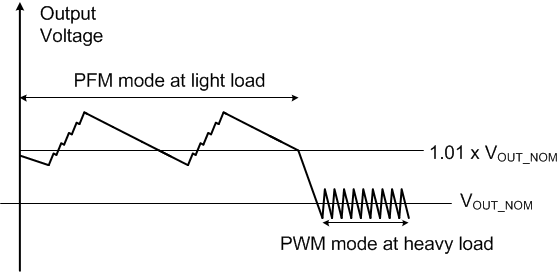
LP5811 Output
                    Voltage in PWM Mode and PFM Figure 6-2 Output Voltage in PWM Mode and PFM