SNVS798P April   2012  – January 2024 LP5907

PRODUCTION DATA  

  1.   1
  2. Features
  3. Applications
  4. Description
  5. Pin Configuration and Functions
  6. Specifications
    1. 5.1 Absolute Maximum Ratings
    2. 5.2 ESD Ratings
    3. 5.3 Recommended Operating Conditions
    4. 5.4 Thermal Information
    5. 5.5 Electrical Characteristics
    6. 5.6 Output and Input Capacitors
    7. 5.7 Typical Characteristics
  7. Detailed Description
    1. 6.1 Overview
    2. 6.2 Functional Block Diagram
    3. 6.3 Feature Description
      1. 6.3.1 Enable (EN)
      2. 6.3.2 Low Output Noise
      3. 6.3.3 Output Automatic Discharge
      4. 6.3.4 Remote Output Capacitor Placement
      5. 6.3.5 Thermal Overload Protection (TSD)
    4. 6.4 Device Functional Modes
      1. 6.4.1 Enable (EN)
      2. 6.4.2 Minimum Operating Input Voltage (VIN)
  8. Application and Implementation
    1. 7.1 Application Information
    2. 7.2 Typical Application
      1. 7.2.1 Design Requirements
      2. 7.2.2 Detailed Design Procedure
        1. 7.2.2.1 Custom Design With WEBENCH® Tools
        2. 7.2.2.2 Power Dissipation and Device Operation
        3. 7.2.2.3 External Capacitors
        4. 7.2.2.4 Input Capacitor
        5. 7.2.2.5 Output Capacitor
        6. 7.2.2.6 Capacitor Characteristics
        7. 7.2.2.7 Remote Capacitor Operation
        8. 7.2.2.8 No-Load Stability
        9. 7.2.2.9 Enable Control
      3. 7.2.3 Application Curves
    3. 7.3 Power Supply Recommendations
    4. 7.4 Layout
      1. 7.4.1 Layout Guidelines
        1. 7.4.1.1 X2SON Mounting
        2. 7.4.1.2 DSBGA Mounting
        3. 7.4.1.3 DSBGA Light Sensitivity
      2. 7.4.2 Layout Examples
  9. Device and Documentation Support
    1. 8.1 Documentation Support
      1. 8.1.1 Custom Design With WEBENCH® Tools
      2. 8.1.2 Related Documentation
    2. 8.2 Receiving Notification of Documentation Updates
    3. 8.3 Support Resources
    4. 8.4 Trademarks
    5. 8.5 Electrostatic Discharge Caution
    6. 8.6 Glossary
  10. Revision History
  11. 10Mechanical, Packaging, and Orderable Information

Package Options

Refer to the PDF data sheet for device specific package drawings

Mechanical Data (Package|Pins)
  • YKM|4
  • DBV|5
  • DQN|4
  • YKG|4
  • YKE|4
Thermal pad, mechanical data (Package|Pins)
Orderable Information

Description

The LP5907 is a low-noise LDO that can supply up to 250mA output current. Designed to meet the requirements of RF and analog circuits, the LP5907 provides low noise, high PSRR, low quiescent current, and low line or load transient response figures. Using innovative design techniques, the LP5907 offers class-leading noise performance without a noise bypass capacitor and the ability for remote output capacitor placement.

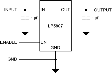
The device is designed to work with a 1µF input and a 1µF output ceramic capacitor (no separate noise bypass capacitor is required).

This device is available with fixed output voltages from 1.2V to 4.5V in 25mV steps. Contact Texas Instruments Sales for specific voltage option needs.

Package Information
PART NUMBER PACKAGE(1) PACKAGE SIZE(2)
LP5907 YKE, YKG, YKM, YCR (DSBGA, 4) 0.685mm × 0.685mm
DBV (SOT-23, 5) 2.9mm × 2.8mm
DQN (X2SON, 4) 1mm × 1mm
For more information, see the Mechanical, Packaging, and Orderable Information.
The package size (length × width) is a nominal value and includes pins, where applicable.
GUID-99FF2F38-4709-4C00-AFA1-1EF35A27F2C0-low.gif Simplified Schematic