SNVS798P April   2012  – January 2024 LP5907

PRODUCTION DATA  

  1.   1
  2. Features
  3. Applications
  4. Description
  5. Pin Configuration and Functions
  6. Specifications
    1. 5.1 Absolute Maximum Ratings
    2. 5.2 ESD Ratings
    3. 5.3 Recommended Operating Conditions
    4. 5.4 Thermal Information
    5. 5.5 Electrical Characteristics
    6. 5.6 Output and Input Capacitors
    7. 5.7 Typical Characteristics
  7. Detailed Description
    1. 6.1 Overview
    2. 6.2 Functional Block Diagram
    3. 6.3 Feature Description
      1. 6.3.1 Enable (EN)
      2. 6.3.2 Low Output Noise
      3. 6.3.3 Output Automatic Discharge
      4. 6.3.4 Remote Output Capacitor Placement
      5. 6.3.5 Thermal Overload Protection (TSD)
    4. 6.4 Device Functional Modes
      1. 6.4.1 Enable (EN)
      2. 6.4.2 Minimum Operating Input Voltage (VIN)
  8. Application and Implementation
    1. 7.1 Application Information
    2. 7.2 Typical Application
      1. 7.2.1 Design Requirements
      2. 7.2.2 Detailed Design Procedure
        1. 7.2.2.1 Custom Design With WEBENCH® Tools
        2. 7.2.2.2 Power Dissipation and Device Operation
        3. 7.2.2.3 External Capacitors
        4. 7.2.2.4 Input Capacitor
        5. 7.2.2.5 Output Capacitor
        6. 7.2.2.6 Capacitor Characteristics
        7. 7.2.2.7 Remote Capacitor Operation
        8. 7.2.2.8 No-Load Stability
        9. 7.2.2.9 Enable Control
      3. 7.2.3 Application Curves
    3. 7.3 Power Supply Recommendations
    4. 7.4 Layout
      1. 7.4.1 Layout Guidelines
        1. 7.4.1.1 X2SON Mounting
        2. 7.4.1.2 DSBGA Mounting
        3. 7.4.1.3 DSBGA Light Sensitivity
      2. 7.4.2 Layout Examples
  9. Device and Documentation Support
    1. 8.1 Documentation Support
      1. 8.1.1 Custom Design With WEBENCH® Tools
      2. 8.1.2 Related Documentation
    2. 8.2 Receiving Notification of Documentation Updates
    3. 8.3 Support Resources
    4. 8.4 Trademarks
    5. 8.5 Electrostatic Discharge Caution
    6. 8.6 Glossary
  10. Revision History
  11. 10Mechanical, Packaging, and Orderable Information

Package Options

Refer to the PDF data sheet for device specific package drawings

Mechanical Data (Package|Pins)
  • YKM|4
  • DBV|5
  • DQN|4
  • YKG|4
  • YKE|4
Thermal pad, mechanical data (Package|Pins)
Orderable Information

Typical Application

Figure 7-1 shows the typical application circuit for the LP5907. Input and output capacitances can be increased, if needed, above the 1µF minimum for some applications.
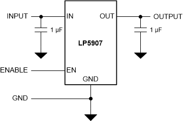
GUID-99FF2F38-4709-4C00-AFA1-1EF35A27F2C0-low.gifFigure 7-1 LP5907 Typical Application