SNVS871M July   2012  – June 2020 LP8556

PRODUCTION DATA.  

  1. Features
  2. Applications
    1.     Simplified Schematic
  3. Description
  4. Revision History
  5. Device Options
  6. Pin Configuration and Functions
    1.     Pin Functions
  7. Specifications
    1. 7.1  Absolute Maximum Ratings
    2. 7.2  ESD Ratings
    3. 7.3  Recommended Operating Conditions
    4. 7.4  Thermal Information
    5. 7.5  Electrical Characteristics
    6. 7.6  Electrical Characteristics — Boost Converter
    7. 7.7  Electrical Characteristics — LED Driver
    8. 7.8  Electrical Characteristics — PWM Interface
    9. 7.9  Electrical Characteristics — Logic Interface
    10. 7.10 I2C Serial Bus Timing Parameters (SDA, SCL)
    11. 7.11 Typical Characteristics
  8. Detailed Description
    1. 8.1 Overview
    2. 8.2 Functional Block Diagram
    3. 8.3 Feature Description
      1. 8.3.1 Boost Converter
        1. 8.3.1.1 Boost Converter Operation
        2. 8.3.1.2 Setting Boost Switching Frequency
        3. 8.3.1.3 Output Voltage Control
          1. 8.3.1.3.1 Adaptive Control
          2. 8.3.1.3.2 Manual Control
        4. 8.3.1.4 EMI Reduction
      2. 8.3.2 Brightness Control
        1. 8.3.2.1  BRT_MODE = 00
        2. 8.3.2.2  BRT_MODE = 01
        3. 8.3.2.3  BRT_MODE = 10
        4. 8.3.2.4  BRT_MODE = 11
        5. 8.3.2.5  Output Dimming Schemes
          1. 8.3.2.5.1 PWM Control
          2. 8.3.2.5.2 Pure Current Control
          3. 8.3.2.5.3 Adaptive Control
        6. 8.3.2.6  Setting Full-Scale LED Current
        7. 8.3.2.7  Setting PWM Dimming Frequency
        8. 8.3.2.8  Phase Shift PWM Scheme
        9. 8.3.2.9  Slope and Advanced Slope
        10. 8.3.2.10 Dithering
      3. 8.3.3 Fault Detection
        1. 8.3.3.1 LED Fault Detection
          1. 8.3.3.1.1 Open Detect
          2. 8.3.3.1.2 Short Detect
        2. 8.3.3.2 Undervoltage Detection
        3. 8.3.3.3 Overcurrent Protection
        4. 8.3.3.4 Thermal Shutdown
    4. 8.4 Device Functional Modes
      1. 8.4.1 Shutdown Mode
      2. 8.4.2 Active Mode
    5. 8.5 Programming
      1. 8.5.1 I2C-Compatible Serial Bus Interface
        1. 8.5.1.1 Interface Bus Overview
        2. 8.5.1.2 Data Transactions
        3. 8.5.1.3 Acknowledge Cycle
        4. 8.5.1.4 Acknowledge After Every Byte Rule
        5. 8.5.1.5 Addressing Transfer Formats
        6. 8.5.1.6 Control Register Write Cycle
        7. 8.5.1.7 Control Register Read Cycle
        8. 8.5.1.8 Register Read and Write Detail
    6. 8.6 Register Maps
      1. 8.6.1 Register Bit Explanations
        1. 8.6.1.1 Brightness Control
        2. 8.6.1.2 Device Control
        3. 8.6.1.3 Status
        4. 8.6.1.4 Direct Control
        5. 8.6.1.5 LED String Enable
      2. 8.6.2 EPROM Bit Explanations
        1. 8.6.2.1  LP8556TM (DSBGA) Configurations and Pre-Configured EPROM Settings
        2. 8.6.2.2  LP8556TM (DSBGA) Configurations and Pre-configured EPROM Settings Continued
        3. 8.6.2.3  LP8556SQ (WQFN) Configurations and Pre-configured EPROM Settings
        4. 8.6.2.4  CFG98
        5. 8.6.2.5  CFG9E
        6. 8.6.2.6  CFG0
        7. 8.6.2.7  CFG1
        8. 8.6.2.8  CFG2
        9. 8.6.2.9  CFG3
        10. 8.6.2.10 CFG4
        11. 8.6.2.11 CFG5
        12. 8.6.2.12 CFG6
        13. 8.6.2.13 CFG7
        14. 8.6.2.14 CFG9
        15. 8.6.2.15 CFGA
        16. 8.6.2.16 CFGE
        17. 8.6.2.17 CFGF
  9. Application and Implementation
    1. 9.1 Application Information
      1. 9.1.1 Using LP8556 With I2C Host
        1. 9.1.1.1 Setting Boost Switching and PWM Dimming Frequencies
        2. 9.1.1.2 Setting Full-Scale LED Current
      2. 9.1.2 Using LP8556 With Configuration Resistors and IO Pins
        1. 9.1.2.1 Setting Boost Switching and PWM Dimming Frequencies
        2. 9.1.2.2 Setting Full-Scale LED Current
    2. 9.2 Typical Application
      1. 9.2.1 Design Requirements
      2. 9.2.2 Detailed Design Procedure
        1. 9.2.2.1 Recommended Inductance for the Boost Power Stage
        2. 9.2.2.2 Recommended Capacitances for the Boost and LDO Power Stages
      3. 9.2.3 Application Curves
  10. 10Power Supply Recommendations
  11. 11Layout
    1. 11.1 Layout Guidelines
    2. 11.2 Layout Examples
  12. 12Device and Documentation Support
    1. 12.1 Receiving Notification of Documentation Updates
    2. 12.2 Community Resources
    3. 12.3 Trademarks
    4. 12.4 Electrostatic Discharge Caution
    5. 12.5 Glossary
  13. 13Mechanical, Packaging, and Orderable Information

Package Options

Mechanical Data (Package|Pins)
Thermal pad, mechanical data (Package|Pins)
Orderable Information

Boost Converter Operation

The LP8556 boost DC-DC converter generates a 7-V to approximately 43-V of boost output voltage from a 2.7-V to 36-V boost input voltage. The boost output voltage minimum, maximum value and range can be set digitally by pre-configuring EPROM memory (VBOOST_RANGE, VBOOST, and VBOOST_MAX fields).

The converter is a magnetic switching PWM mode DC-DC boost converter with a current limit. It uses CPM (current programmed mode) control, where the inductor current is measured and controlled with the feedback. During start-up, the soft-start function reduces the peak inductor current. The LP8556 has an internal 20-MHz oscillator which is used for clocking the boost. Figure 4 shows the boost block diagram.
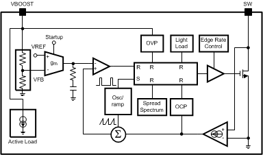
LP8556 30162640.gifFigure 4. LP8556 Boost Converter Block Diagram