SNVS871M July 2012 – June 2020 LP8556
PRODUCTION DATA.
- 1 Features
- 2 Applications
- 3 Description
- 4 Revision History
- 5 Device Options
- 6 Pin Configuration and Functions
-
7 Specifications
- 7.1 Absolute Maximum Ratings
- 7.2 ESD Ratings
- 7.3 Recommended Operating Conditions
- 7.4 Thermal Information
- 7.5 Electrical Characteristics
- 7.6 Electrical Characteristics — Boost Converter
- 7.7 Electrical Characteristics — LED Driver
- 7.8 Electrical Characteristics — PWM Interface
- 7.9 Electrical Characteristics — Logic Interface
- 7.10 I2C Serial Bus Timing Parameters (SDA, SCL)
- 7.11 Typical Characteristics
-
8 Detailed Description
- 8.1 Overview
- 8.2 Functional Block Diagram
- 8.3
Feature Description
- 8.3.1 Boost Converter
- 8.3.2 Brightness Control
- 8.3.3 Fault Detection
- 8.4 Device Functional Modes
- 8.5 Programming
- 8.6
Register Maps
- 8.6.1 Register Bit Explanations
- 8.6.2
EPROM Bit Explanations
- 8.6.2.1 LP8556TM (DSBGA) Configurations and Pre-Configured EPROM Settings
- 8.6.2.2 LP8556TM (DSBGA) Configurations and Pre-configured EPROM Settings Continued
- 8.6.2.3 LP8556SQ (WQFN) Configurations and Pre-configured EPROM Settings
- 8.6.2.4 CFG98
- 8.6.2.5 CFG9E
- 8.6.2.6 CFG0
- 8.6.2.7 CFG1
- 8.6.2.8 CFG2
- 8.6.2.9 CFG3
- 8.6.2.10 CFG4
- 8.6.2.11 CFG5
- 8.6.2.12 CFG6
- 8.6.2.13 CFG7
- 8.6.2.14 CFG9
- 8.6.2.15 CFGA
- 8.6.2.16 CFGE
- 8.6.2.17 CFGF
- 9 Application and Implementation
- 10Power Supply Recommendations
- 11Layout
- 12Device and Documentation Support
- 13Mechanical, Packaging, and Orderable Information
Package Options
Mechanical Data (Package|Pins)
Thermal pad, mechanical data (Package|Pins)
- RTW|24
Orderable Information
8.3.1.4 EMI Reduction
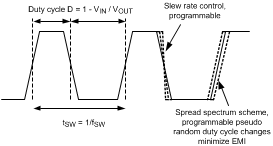
The LP8556 device features two EMI reduction schemes.
The first scheme, Programmable Slew Rate Control, uses a combination of three drivers for boost switch. Enabling all three drivers allows boost switch on/off transition times to be the shortest. On the other hand, enabling just one driver allows boost switch on/off transition times to be the longest. The longer the transition times, the lower the switching noise on the SW pin. Note that the shortest transition times bring the best efficiency as the switching losses are the lowest.
EN_DRV2 and EN_DRV3 bits in the EPROM determine the boost switch driver configuration. Refer to the SW pin slew rate parameter listed under Electrical Characteristics — Boost Converter for the slew rate options.
The second EMI reduction scheme is the spread spectrum. This scheme deliberately spreads the frequency content of the boost switching waveform, which inherently has a narrow bandwidth, makes the bandwidth of the switching waveform wider, and ultimately reduces its EMI spectral density.
 Figure 6. Principles of EMI Reduction Scheme