SNVSA71 February 2015 LP8728C-Q1
PRODUCTION DATA.
- 1 Features
- 2 Applications
- 3 Description
- 4 Revision History
- 5 Pin Configuration and Functions
- 6 Specifications
- 7 Detailed Description
- 8 Application and Implementation
- 9 Power Supply Recommendations
- 10Layout
- 11Device and Documentation Support
- 12Mechanical, Packaging, and Orderable Information
Package Options
Mechanical Data (Package|Pins)
- RSG|28
Thermal pad, mechanical data (Package|Pins)
- RSG|28
Orderable Information
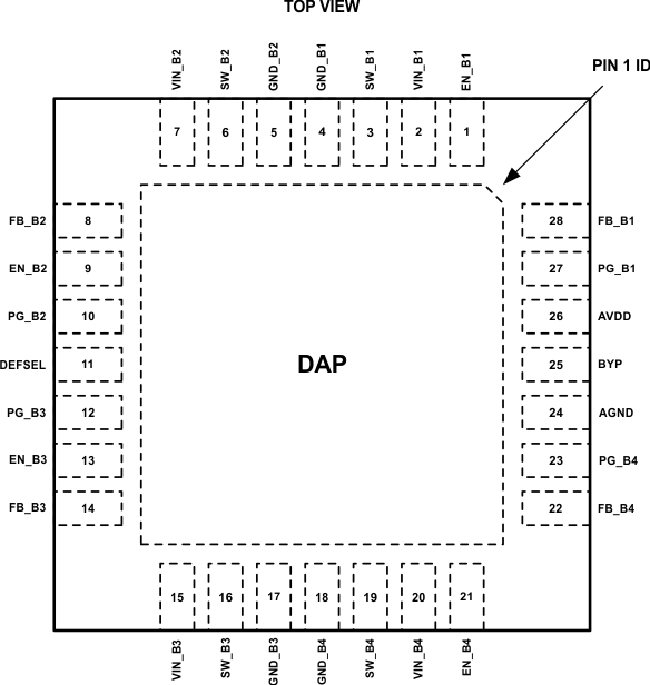
5 Pin Configuration and Functions
WQFN (RSG) Package
28 Pins

Pin Functions
| PIN | TYPE(1) | DESCRIPTION | |
|---|---|---|---|
| NUMBER | NAME | ||
| 1 | EN_B1 | D/I | Enable Buck 1 |
| 2 | VIN_B1 | P | Positive power supply input for Buck 1 |
| 3 | SW_B1 | P | Switch node for Buck 1 |
| 4 | GND_B1 | G | Power ground for Buck 1 |
| 5 | GND_B2 | G | Power ground for Buck 2 |
| 6 | SW_B2 | P | Switch node for Buck 2 |
| 7 | VIN_B2 | P | Positive power supply input for Buck 2 |
| 8 | FB_B2 | A | Feedback pin for Buck 2. Referenced against AGND. |
| 9 | EN_B2 | D/I | Enable Buck 2 |
| 10 | PG_B2 | D/O | Open-drain Power Good output for Buck 2 |
| 11 | DEFSEL | D/I | Buck 3 output voltage selection pin |
| 12 | PG_B3 | D/O | Open-drain Power Good output for Buck 3 |
| 13 | EN_B3 | D/I | Enable Buck 3 |
| 14 | FB_B3 | A | Feedback pin for Buck 3. Referenced against AGND. |
| 15 | VIN_B3 | P | Positive power supply input for Buck 3 |
| 16 | SW_B3 | P | Switch node for Buck 3 |
| 17 | GND_B3 | G | Power ground for Buck 3 |
| 18 | GND_B4 | G | Power ground for Buck 4 |
| 19 | SW_B4 | P | Switch node for Buck 4 |
| 20 | VIN_B4 | P | Positive power supply input for Buck 4 |
| 21 | EN_B4 | D/I | Enable Buck 4 |
| 22 | FB_B4 | A | Feedback pin for Buck 4. Referenced against AGND. |
| 23 | PG_B4 | D/O | Open-drain Power Good output for Buck 4 |
| 24 | AGND | G | Analog ground |
| 25 | BYP | A | Internal 1.8-V supply voltage capacitor pin. A ceramic low-ESR 1-μF capacitor should be connected from this pin to AGND. The BYP voltage is generated internally, do not supply or load this pin externally. |
| 26 | AVDD | P | Analog positive power supply pin (VIN level) |
| 27 | PG_B1 | D/O | Open-drain Power Good output for Buck 1 |
| 28 | FB_B1 | A | Feedback pin for Buck 1. Referenced against AGND. |
| DAP | Die Attachment Pad | Exposed die attachment pad should to be connected to GND plane with thermal vias to improve the thermal performance of the system. | |
(1) A: Analog Pin, G: Ground Pin, P: Power Pin, O: Output Pin, D/I: Digital Input, D/O: Digital Output.