SNVSA72 February 2015 LP8728D-Q1
PRODUCTION DATA.
- 1 Features
- 2 Applications
- 3 Description
- 4 Revision History
- 5 Pin Configuration and Functions
- 6 Specifications
- 7 Detailed Description
- 8 Application and Implementation
- 9 Power Supply Recommendations
- 10Layout
- 11Device and Documentation Support
- 12Mechanical, Packaging, and Orderable Information
Package Options
Mechanical Data (Package|Pins)
- RSG|28
Thermal pad, mechanical data (Package|Pins)
- RSG|28
Orderable Information
6 Specifications
6.1 Absolute Maximum Ratings
over operating free-air temperature range (unless otherwise noted)(1)| MIN | MAX | UNIT | ||
|---|---|---|---|---|
| VIN | Voltage on power pins (AVDD, VIN_Bx) | –0.3 | 6 | V |
| VFB | Voltage on feedback pins (FB_Bx) | –0.3 | 6 | V |
| VSW | Voltage on buck converter switch pins (SW_Bx) | (GND_Bx – 0.2 V) to (VIN_Bx + 0.2 V) with 6 V max | V | |
| VDIG | Voltage on digital pins (PG_Bx, EN_Bx, DEFSEL) | (AGND – 0.2V) to (AVDD + 0.2 V) with 6 V max | V | |
| VBYP | Voltage on BYP pin | –0.3 | 2 | V |
| TJ(MAX) | Maximum operating junction temperature(2) | 150 | °C | |
| Maximum lead temperature (Soldering) | See(3) | |||
| Tstg | Storage temperature | –65 | 150 | °C |
(1) Stresses beyond those listed under Absolute Maximum Ratings may cause permanent damage to the device. These are stress ratings only, which do not imply functional operation of the device at these or any other conditions beyond those indicated under Recommended Operating Conditions. Exposure to absolute-maximum-rated conditions for extended periods may affect device reliability.
(2) Internal thermal shutdown circuitry protects the device from permanent damage. Thermal shutdown engages at TJ = 150°C (typical) and disengages at TJ = 130°C (typical).
(3) For detailed soldering specifications and information, please refer to Texas Instruments Application Note Leadless Leadframe Package (LLP)SNOA401.
6.2 ESD Ratings
| VALUE | UNIT | |||
|---|---|---|---|---|
| V(ESD) | Electrostatic discharge | Human-body model (HBM), per AEC Q100-002(1) | ±2000 | V |
| Charged-device model (CDM), per AEC Q100-011 | ±750 | |||
(1) AEC Q100-002 indicates that HBM stressing shall be in accordance with the ANSI/ESDA/JEDEC JS-001 specification.
6.3 Recommended Operating Conditions
over operating free-air temperature range (unless otherwise noted)(1)| MIN | NOM | MAX | UNIT | ||
|---|---|---|---|---|---|
| VIN | Input voltage on AVDD, VIN_B1, VIN_B2, VIN_B3 and VIN_B4 pins | 4.5 | 5 | 5.5 | V |
| TA | Operating ambient temperature(2) | –40 | 125 | °C | |
| COUT | Effective output capacitance during operation. Min value over TA –40°C to 125°C. |
5 | 10 | 12 | µF |
| CIN | Effective input capacitance during operation. 4.5 V ≤ VIN_Bx ≤ 5.5 V. Min value over TA –40°C to 125°C. |
2.5 | 10 | µF | |
| L | Effective inductance during operation Min value over TA –40°C to 125°C. |
0.47 | 1.5 | 2 | µF |
(1) All voltage values are with respect to network ground terminal.
(2) In applications where high power dissipation and/or poor package thermal resistance is present, the maximum ambient temperature may have to be derated. Maximum ambient temperature (TA(max)) is dependent on the maximum operating junction temperature (TJ(max)), the maximum power dissipation of the device in the application (PD(max)), and the junction-to-ambient thermal resistance of the part/package in the application (RθJA), as given by the following equation: TA(max) = TJ(max) – (RθJA × PD(max))
6.4 Thermal Information
| THERMAL METRIC(1) | LP8728-Q1 | UNIT | |
|---|---|---|---|
| WQFN (RSG) | |||
| 28 PINS | |||
| RθJA | Junction-to-ambient thermal resistance(2) | 37.7 | °C/W |
| RθJCtop | Junction-to-case (top) thermal resistance | 24.5 | |
| RθJB | Junction-to-board thermal resistance | 10.8 | |
| ΨJT | Junction-to-top characterization parameter | 0.3 | |
| ΨJB | Junction-to-board characterization parameter | 10.8 | |
| RθJCbot | Junction-to-case (bottom) thermal resistance | 2.7 | |
(1) For more information about traditional and new thermal metrics, see the IC Package Thermal Metrics application report, SPRA953.
(2) Calculated using 4-layer standard JEDEC thermal test board with 5 thermal vias between the die attach pad in the first copper layer and second copper layer.
6.5 Electrical Characteristics(1)(2)
Unless otherwise noted, VIN = 5 V, typical values apply for TA = 25°C, and minimum/maximum limits apply over junction temperature range, TJ = –40°C to 125°C.| PARAMETER | TEST CONDITIONS | MIN | TYP | MAX | UNIT | |
|---|---|---|---|---|---|---|
| ISHDN | Shutdown supply current into power connections | EN_Bx = 0 V | 1 | 6 | μA | |
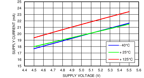
| IOP | Operating current | All buck-converters active, IOUT = 0 mA | 20 | mA | ||
| LOGIC INPUTS (EN_Bx, DEFSEL) | ||||||
| VIL | Input low level | 0.4 | V | |||
| VIH | Input high level | 1.6 | V | |||
| RPD_DI | EN_Bx and DEFSEL internal pulldown resistance | 300 | 520 | 820 | kΩ | |
| TH_MIN | Minimum EN_Bx high time | 1 | ms | |||
| TL_MIN | Minimum EN_Bx low time | 10 | µs | |||
| LOGIC OUTPUTS (PG_Bx) | ||||||
| VOL | Output low level | ISINK = 3 mA | 0.4 | V | ||
| RPU | Recommended pullup resistor | 10 | kΩ | |||
| BUCK CONVERTERS | ||||||
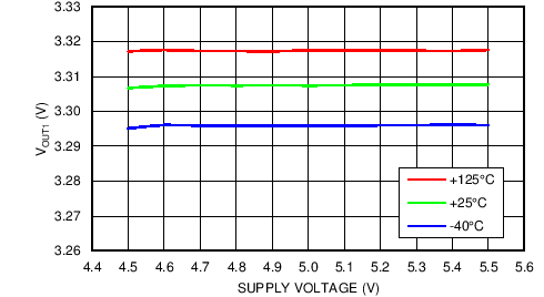
| VOUT1 | Output voltage for Buck 1 | Fixed voltage | 3.3 | V | ||
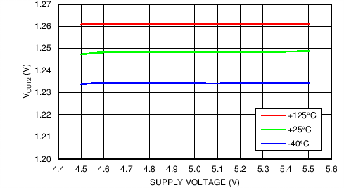
| VOUT2 | Output voltage for Buck 2 | Fixed voltage | 1.25 | V | ||
| VOUT3 | Output voltage for Buck 3 | DEFSEL = 1 | 2.65 | V | ||
| DEFSEL = 0 | 1.8 | |||||
| VOUT4 | Output voltage for Buck 4 | Fixed voltage | 1.8 | V | ||
| VFB_Bx | Output voltage accuracy | –3% | 3% | |||
| ΔVOUT | Line regulation | 4.5 V ≤ VIN_Bx ≤ 5.5 V, ILOAD = 10 mA | 3 | mV | ||
| Load regulation | VIN = 5 V, 100 mA ≤ ILOAD ≤ 900 mA | 3 | mV | |||
| IOUT | Output current | DC load TA = 25°C |
1000 | mA | ||
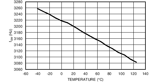
| fSW | Switching frequency | 3.03 | 3.2 | 3.37 | MHz | |
| GBW | Gain bandwidth | 300 | kHz | |||
| ILIMITP | High-side switch current limit | 1200 | 1500 | 1800 | mA | |
| ILIMITN | Low-side switch current limit | Reverse current | 500 | mA | ||
| RDSONP | Pin-pin resistance for PFET | IOUT = 200 mA | 210 | 300 | mΩ | |
| RDSONN | Pin-pin resistance for NFET | IOUT = 200 mA | 140 | 240 | mΩ | |
| ILK_SW | Switch pin leakage current | VOUT = 1.8V | 1 | µA | ||
| RPD_FB | Pulldown resistor from FB_Bx pin to GND | Only active when converter disabled. All limits apply for TA = 25°C |
40 | 70 | 100 | Ω |
| KRAMP | Slew rate control | DEFSEL from 0 to 1 | 10 | mV/µs | ||
| TSTART | Start-up time | Time from first EN_Bx high to start of switching | 420 | µs | ||
| KSTART | Soft-start VOUT slew rate | 18 | mV/µs | |||
| VOLTAGE MONITORING | ||||||
| VPG | Power good threshold voltage | Power good threshold for voltage rising | 93.5% | 96% | 98% | |
| Power good threshold for voltage falling | 91% | 93% | 95% | |||
| VOVP | Input overvoltage protection trigger point | Voltage monitored on AVDD Pin, voltage rising | 5.5 | 5.7 | 5.9 | V |
| Hysteresis | 80 | mV | ||||
| VUVLO | Input undervoltage lockout (UVLO) threshold. | Voltage monitored on AVDD Pin, voltage falling | 2.7 | V | ||
| Hysteresis | 80 | mV | ||||
| THERMAL SHUTDOWN AND MONITORING | ||||||
| TSD | Thermal shutdown | Threshold, temperature rising | 150 | °C | ||
| Hysteresis | 20 | |||||
(1) All voltage values are with respect to network ground terminal.
(2) Minimum (Min) and Maximum (Max) limits are specified by design, test, or statistical analysis. Typical (Typ) numbers are not verified, but do represent the most likely norm. Unless otherwise specified, conditions for Typ specifications are: VIN = 5 V and TJ = 25°C.
6.6 System Characteristics(1)(2)(3)
Typical values apply for TA = 25°C. Unless otherwise noted, VIN = 5 V.| PARAMETER | TEST CONDITIONS | MIN | TYP | MAX | UNIT | |
|---|---|---|---|---|---|---|
| ΔVOUT | Load transient response | IOUT 10% max load → 90% max load, 1-µs load step | 70 | mV | ||
| IOUT 90% max load → 10% max load, 1-µs load step | 70 | mV | ||||
| Line transient response | VIN_Bx stepping 4.5 V ↔ 5.5 V, tRISE = tFALL = 10 µs, IOUT = 400 mA | 20 | mV | |||
| VRIPPLE | Output voltage ripple | COUT ESR = 10 mΩ, IOUT = 200 mA | 10 | mVPP | ||
| η | Efficiency | VOUT = 3.3 V, IOUT = 300 mA | 94% | |||
| VOUT = 2.65 V, IOUT = 300 mA | 92% | |||||
| VOUT = 1.8 V, IOUT = 300 mA | 89% | |||||
| VOUT = 1.25 V, IOUT = 300 mA | 85% | |||||
(1) All voltage values are with respect to network ground terminal.
(2) Minimum (Min) and Maximum (Max) limits are specified by design, test, or statistical analysis. Typical (Typ) numbers are not verified, but do represent the most likely norm. Unless otherwise specified, conditions for Typ specifications are: VIN = 5 V and TJ = 25°C.
(3) System Characteristics are highly dependent on external components and PCB layout. System Characteristics are verified using inductor type: TOKO MDT2520-CN1R5M, input and output capacitor type: MuRata GRM21BR71A106KE51L.
6.7 Typical Characteristics
Unless otherwise noted, VIN = 5 V, TA = 25°C, inductor type: TOKO MDT2520-CN1R5M, input and output capacitor type: MuRata GRM21BR71A106KE51L.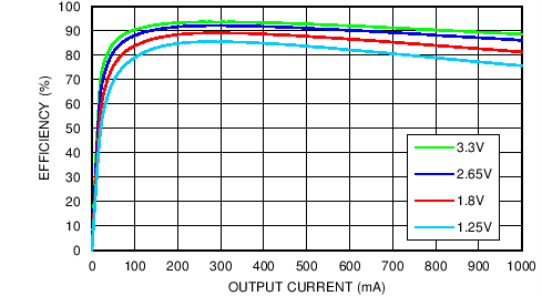
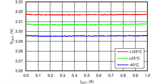
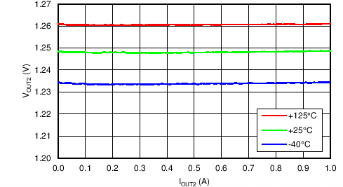
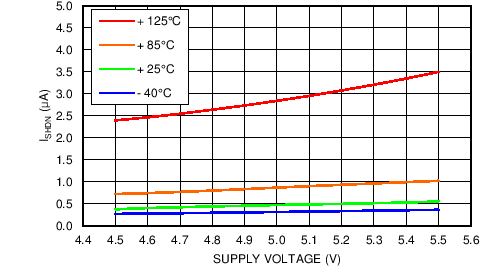
(All Bucks Active)