SNVSAU7A November 2017 – June 2021 LP873220
PRODUCTION DATA
- 1 Features
- 2 Applications
- 3 Description
- 4 Revision History
- 5 Pin Configuration and Functions
- 6 Specifications
-
7 Detailed Description
- 7.1 Overview
- 7.2 Functional Block Diagram
- 7.3
Feature Description
- 7.3.1 DC/DC Converters
- 7.3.2 Sync Clock Functionality
- 7.3.3 Low-Dropout Linear Regulators (LDOs)
- 7.3.4 Power-Up
- 7.3.5 Regulator Control
- 7.3.6 Enable and Disable Sequences
- 7.3.7 Device Reset Scenarios
- 7.3.8 Diagnosis and Protection Features
- 7.3.9 Operation of the GPO Signals
- 7.3.10 Digital Signal Filtering
- 7.4 Device Functional Modes
- 7.5 Programming
- 7.6
Register Maps
- 7.6.1
Register Descriptions
- 7.6.1.1 DEV_REV
- 7.6.1.2 OTP_REV
- 7.6.1.3 BUCK0_CTRL_1
- 7.6.1.4 BUCK0_CTRL_2
- 7.6.1.5 BUCK1_CTRL_1
- 7.6.1.6 BUCK1_CTRL_2
- 7.6.1.7 BUCK0_VOUT
- 7.6.1.8 BUCK1_VOUT
- 7.6.1.9 LDO0_CTRL
- 7.6.1.10 LDO1_CTRL
- 7.6.1.11 LDO0_VOUT
- 7.6.1.12 LDO1_VOUT
- 7.6.1.13 BUCK0_DELAY
- 7.6.1.14 BUCK1_DELAY
- 7.6.1.15 LDO0_DELAY
- 7.6.1.16 LDO1_DELAY
- 7.6.1.17 GPO_DELAY
- 7.6.1.18 GPO2_DELAY
- 7.6.1.19 GPO_CTRL
- 7.6.1.20 CONFIG
- 7.6.1.21 PLL_CTRL
- 7.6.1.22 PGOOD_CTRL_1
- 7.6.1.23 PGOOD_CTRL_2
- 7.6.1.24 PG_FAULT
- 7.6.1.25 RESET
- 7.6.1.26 INT_TOP_1
- 7.6.1.27 INT_TOP_2
- 7.6.1.28 INT_BUCK
- 7.6.1.29 INT_LDO
- 7.6.1.30 TOP_STAT
- 7.6.1.31 BUCK_STAT
- 7.6.1.32 LDO_STAT
- 7.6.1.33 TOP_MASK_1
- 7.6.1.34 TOP_MASK_2
- 7.6.1.35 BUCK_MASK
- 7.6.1.36 LDO_MASK
- 7.6.1.37 SEL_I_LOAD
- 7.6.1.38 I_LOAD_2
- 7.6.1.39 I_LOAD_1
- 7.6.1
Register Descriptions
- 8 Application and Implementation
- 9 Power Supply Recommendations
- 10Layout
- 11Device and Documentation Support
- 12Mechanical, Packaging, and Orderable Information
Package Options
Mechanical Data (Package|Pins)
- RHD|28
Thermal pad, mechanical data (Package|Pins)
- RHD|28
Orderable Information
7.3.2 Sync Clock Functionality
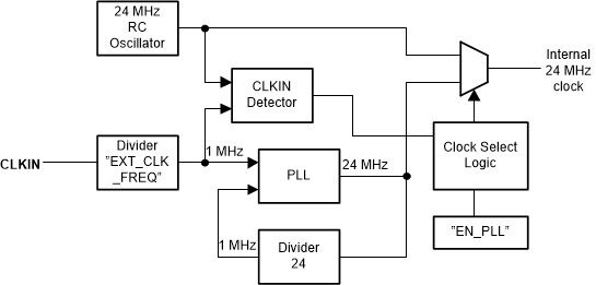
The LP873220 device contains a CLKIN input to synchronize the switching clock of the buck regulators with the external clock. The block diagram of the clocking and PLL module is shown in Figure 7-3. Depending on the EN_PLL bit in the PLL_CTRL register and the external clock availability, the external clock is selected and interrupt is generated as shown in Table 7-2. The interrupt can be masked with the SYNC_CLK_MASK bit in the TOP_MASK_1 register. The nominal frequency of the external input clock is set by the EXT_CLK_FREQ[4:0] bits in the PLL_CTRL register, and it can be from 1 MHz to 24 MHz with 1-MHz steps. The external clock must be inside accuracy limits (–30%/+10%) of the selected frequency for valid clock detection.
The SYNC_CLK_INT interrupt in the INT_TOP_1 register is also generated in cases where the external clock is expected but is not available. These cases occur when EN_PLL is 1 during start-up (read OTP-to-standby transition) and during Buck regulator enable (standby-to-active transition).
 Figure 7-3 Clock and PLL Module
| DEVICE OPERATION MODE | EN_PLL | PLL AND CLOCK DETECTOR STATE | INTERRUPT FOR EXTERNAL CLOCK | CLOCK |
|---|---|---|---|---|
| STANDBY | 0 | Disabled | No | Internal RC |
| ACTIVE | 0 | Disabled | No | Internal RC |
| STANDBY | 1 | Enabled | When external clock appears or disappears | Automatic change to external clock when available |
| ACTIVE | 1 | Enabled | When external clock appears or disappears | Automatic change to external clock when available |