SNVSAU7A November 2017 – June 2021 LP873220
PRODUCTION DATA
- 1 Features
- 2 Applications
- 3 Description
- 4 Revision History
- 5 Pin Configuration and Functions
- 6 Specifications
-
7 Detailed Description
- 7.1 Overview
- 7.2 Functional Block Diagram
- 7.3
Feature Description
- 7.3.1 DC/DC Converters
- 7.3.2 Sync Clock Functionality
- 7.3.3 Low-Dropout Linear Regulators (LDOs)
- 7.3.4 Power-Up
- 7.3.5 Regulator Control
- 7.3.6 Enable and Disable Sequences
- 7.3.7 Device Reset Scenarios
- 7.3.8 Diagnosis and Protection Features
- 7.3.9 Operation of the GPO Signals
- 7.3.10 Digital Signal Filtering
- 7.4 Device Functional Modes
- 7.5 Programming
- 7.6
Register Maps
- 7.6.1
Register Descriptions
- 7.6.1.1 DEV_REV
- 7.6.1.2 OTP_REV
- 7.6.1.3 BUCK0_CTRL_1
- 7.6.1.4 BUCK0_CTRL_2
- 7.6.1.5 BUCK1_CTRL_1
- 7.6.1.6 BUCK1_CTRL_2
- 7.6.1.7 BUCK0_VOUT
- 7.6.1.8 BUCK1_VOUT
- 7.6.1.9 LDO0_CTRL
- 7.6.1.10 LDO1_CTRL
- 7.6.1.11 LDO0_VOUT
- 7.6.1.12 LDO1_VOUT
- 7.6.1.13 BUCK0_DELAY
- 7.6.1.14 BUCK1_DELAY
- 7.6.1.15 LDO0_DELAY
- 7.6.1.16 LDO1_DELAY
- 7.6.1.17 GPO_DELAY
- 7.6.1.18 GPO2_DELAY
- 7.6.1.19 GPO_CTRL
- 7.6.1.20 CONFIG
- 7.6.1.21 PLL_CTRL
- 7.6.1.22 PGOOD_CTRL_1
- 7.6.1.23 PGOOD_CTRL_2
- 7.6.1.24 PG_FAULT
- 7.6.1.25 RESET
- 7.6.1.26 INT_TOP_1
- 7.6.1.27 INT_TOP_2
- 7.6.1.28 INT_BUCK
- 7.6.1.29 INT_LDO
- 7.6.1.30 TOP_STAT
- 7.6.1.31 BUCK_STAT
- 7.6.1.32 LDO_STAT
- 7.6.1.33 TOP_MASK_1
- 7.6.1.34 TOP_MASK_2
- 7.6.1.35 BUCK_MASK
- 7.6.1.36 LDO_MASK
- 7.6.1.37 SEL_I_LOAD
- 7.6.1.38 I_LOAD_2
- 7.6.1.39 I_LOAD_1
- 7.6.1
Register Descriptions
- 8 Application and Implementation
- 9 Power Supply Recommendations
- 10Layout
- 11Device and Documentation Support
- 12Mechanical, Packaging, and Orderable Information
Package Options
Mechanical Data (Package|Pins)
- RHD|28
Thermal pad, mechanical data (Package|Pins)
- RHD|28
Orderable Information
5 Pin Configuration and Functions
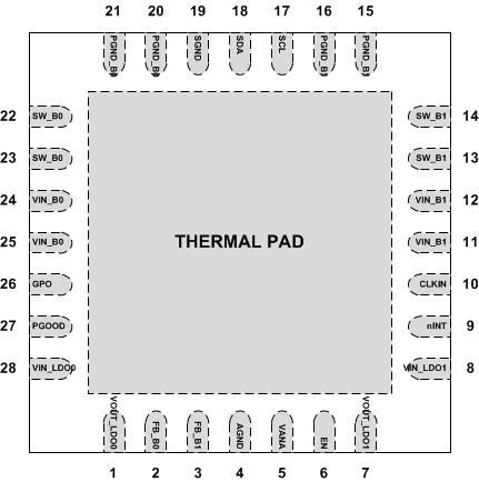
 Figure 5-1 RHD Package28-Pin VQFN With Thermal PadTop View
Table 5-1 Pin Functions
| PIN | TYPE(1) | DESCRIPTION | |
|---|---|---|---|
| NUMBER | NAME | ||
| 1 | VOUT_LDO0 | P/O | LDO0 output. If the LDO0 is not used, leave the pin floating. |
| 2 | FB_B0 | A | Output voltage feedback (positive) for Buck 0. |
| 3 | FB_B1 | A | Output voltage feedback (positive) for Buck 1 |
| 4 | AGND | G | Ground. |
| 5 | VANA | P/I | Supply voltage for analog and digital blocks. Must be connected to same node with VIN_Bx. |
| 6 | EN | D/I | Programmable enable signal for regulators and GPOs. If the pin is not used, leave the pin floating. |
| 7 | VOUT_LDO1 | P/O | LDO1 output. If LDO1 is not used, leave the pin floating. |
| 8 | VIN_LDO1 | P/I | Power input for LDO1. If LDO1 is not used, connect the pin to VANA. |
| 9 | nINT | D/O | Open-drain interrupt output. Active LOW. If the pin is not used, connect the pin to ground. |
| 10 | CLKIN | D/I/O | External clock input. Alternative function is general-purpose digital output (GPO2). If the pin is not used, leave the pin floating. |
| 11, 12 | VIN_B1 | P/I | Input for Buck 1. The separate power pins VIN_Bx are not connected together internally - VIN_Bx pins must be connected together in the application and be locally bypassed. |
| 13, 14 | SW_B1 | P/O | Buck 1 switch node. If the Buck 1 is not used, leave the pin floating. |
| 15, 16 | PGND_B1 | P/G | Power ground for Buck 1. |
| 17 | SCL | D/I | Serial interface clock input for I2C access. Connect a pullup resistor. If the I2C interface is not used, connect the pin to Ground. |
| 18 | SDA | D/I/O | Serial interface data input and output for I2C access. Connect a pullup resistor. If the I2C interface is not used, connect the pin to Ground. |
| 19 | SGND | G | Ground. |
| 20, 21 | PGND_B0 | P/G | Power ground for Buck 0. |
| 22, 23 | SW_B0 | P/O | Buck 0 switch node. If the Buck 0 is not used, leave the pin floating. |
| 24, 25 | VIN_B0 | P/I | Input for Buck 0. The separate power pins VIN_Bx are not connected together internally - VIN_Bx pins must be connected together in the application and be locally bypassed. |
| 26 | GPO | D/O | General-purpose digital output. If the pin is not used, leave the pin floating. |
| 27 | PGOOD | D/O | Power-good indication signal. If the pin is not used, leave the pin floating. |
| 28 | VIN_LDO0 | P/I | Power input for LDO0. If the LDO0 is not used, connect the pin to VANA. |
| Thermal Pad | — | — | Connect to PCB ground plane using multiple vias for good thermal performance. |
(1) A: Analog Pin, D: Digital Pin, G: Ground Pin, P: Power Pin, I: Input
Pin, and O: Output Pin.