SNVSAT3A June 2017 – June 2021 LP873222-Q1
PRODUCTION DATA
- 1 Features
- 2 Applications
- 3 Description
- 4 Revision History
- 5 Pin Configuration and Functions
- 6 Specifications
-
7 Detailed Description
- 7.1 Overview
- 7.2 Functional Block Diagram
- 7.3
Feature Description
- 7.3.1 DC/DC Converters
- 7.3.2 Sync Clock Functionality
- 7.3.3 Low-Dropout Linear Regulators (LDOs)
- 7.3.4 Power-Up
- 7.3.5 Regulator Control
- 7.3.6 Enable and Disable Sequences
- 7.3.7 Device Reset Scenarios
- 7.3.8 Diagnosis and Protection Features
- 7.3.9 Operation of the GPO Signals
- 7.3.10 Digital Signal Filtering
- 7.4 Device Functional Modes
- 7.5 Programming
- 7.6
Register Maps
- 7.6.1
Register Descriptions
- 7.6.1.1 DEV_REV
- 7.6.1.2 OTP_REV
- 7.6.1.3 BUCK0_CTRL_1
- 7.6.1.4 BUCK0_CTRL_2
- 7.6.1.5 BUCK1_CTRL_1
- 7.6.1.6 BUCK1_CTRL_2
- 7.6.1.7 BUCK0_VOUT
- 7.6.1.8 BUCK1_VOUT
- 7.6.1.9 LDO0_CTRL
- 7.6.1.10 LDO1_CTRL
- 7.6.1.11 LDO0_VOUT
- 7.6.1.12 LDO1_VOUT
- 7.6.1.13 BUCK0_DELAY
- 7.6.1.14 BUCK1_DELAY
- 7.6.1.15 LDO0_DELAY
- 7.6.1.16 LDO1_DELAY
- 7.6.1.17 GPO_DELAY
- 7.6.1.18 GPO2_DELAY
- 7.6.1.19 GPO_CTRL
- 7.6.1.20 CONFIG
- 7.6.1.21 PLL_CTRL
- 7.6.1.22 PGOOD_CTRL_1
- 7.6.1.23 PGOOD_CTRL_2
- 7.6.1.24 PG_FAULT
- 7.6.1.25 RESET
- 7.6.1.26 INT_TOP_1
- 7.6.1.27 INT_TOP_2
- 7.6.1.28 INT_BUCK
- 7.6.1.29 INT_LDO
- 7.6.1.30 TOP_STAT
- 7.6.1.31 BUCK_STAT
- 7.6.1.32 LDO_STAT
- 7.6.1.33 TOP_MASK_1
- 7.6.1.34 TOP_MASK_2
- 7.6.1.35 BUCK_MASK
- 7.6.1.36 LDO_MASK
- 7.6.1.37 SEL_I_LOAD
- 7.6.1.38 I_LOAD_2
- 7.6.1.39 I_LOAD_1
- 7.6.1
Register Descriptions
- 8 Application and Implementation
- 9 Power Supply Recommendations
- 10Layout
- 11Device and Documentation Support
- 12Mechanical, Packaging, and Orderable Information
Package Options
Mechanical Data (Package|Pins)
- RHD|28
Thermal pad, mechanical data (Package|Pins)
- RHD|28
Orderable Information
7.3.8.2.1 Output Power Limit
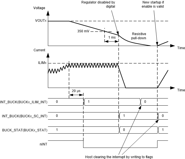
The Buck regulators have programmable output peak current limits. The limits are individually programmed for both regulators with the BUCKx_ILIM[2:0] bits in the BUCKx_CTRL_2 register. If the load current is increased so that the current limit is triggered, then the regulator continues to regulate at the limit current level (peak current regulation). The voltage may decrease if the load current is higher than the limit current. If the current regulation continues for 20 µs, than the LP873222-Q1 device sets the BUCKx_ILIM_INT bit in the INT_BUCK register and pulls the nINT pin low. The host processor can read the BUCKx_ILIM_STAT bits in the BUCK_STAT register to see if the regulator is still in peak current regulation mode, and the interrupt is cleared by writing 1 to the BUCKx_ILIM_INT bit. The current limit interrupt can be masked by setting the BUCKx_ILIM_MASK bit in the BUCK_MASK register to 1. The Buck overload situation is shown in Figure 7-11.
 Figure 7-11 Buck Regulator Overload Situation
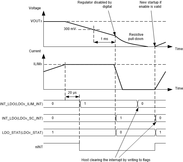
The LDO regulators also include current limit circuitry. If the load current is increased so that the current limit is triggered, the regulator limits the output current to the threshold level. The voltage may decrease if the load current is higher than the current limit. If the current regulation continues for 20 µs, the LP873222-Q1 device sets the LDOx_ILIM_INT bit in the INT_LDO register and pulls the nINT pin low. The host processor can read the LDOx_ILIM_STAT bits in the LDO_STAT register to see if the regulator is still in current regulation mode and the interrupt is cleared by writing 1 to the LDOx_ILIM_INT bit. The current limit interrupt can be masked by setting the LDOx_ILIM_MASK bit in the LDO_MASK register to 1. The LDO overload situation is shown in Figure 7-12.
 Figure 7-12 LDO Regulator Overload Situation