SNVSB64A June 2019 – June 2021 LP8733-Q1
PRODUCTION DATA
- 1 Features
- 2 Applications
- 3 Description
- 4 Revision History
- 5 Pin Configuration and Functions
- 6 Specifications
-
7 Detailed Description
- 7.1 Overview
- 7.2 Functional Block Diagram
- 7.3
Feature Description
- 7.3.1 DC/DC Converters
- 7.3.2 Sync Clock Functionality
- 7.3.3 Low-Dropout Linear Regulators (LDOs)
- 7.3.4 Power-Up
- 7.3.5 Regulator Control
- 7.3.6 Enable and Disable Sequences
- 7.3.7 Device Reset Scenarios
- 7.3.8 Diagnosis and Protection Features
- 7.3.9 Operation of the GPO Signals
- 7.3.10 Digital Signal Filtering
- 7.4 Device Functional Modes
- 7.5 Programming
- 7.6
Register Maps
- 7.6.1
Register Descriptions
- 7.6.1.1 DEV_REV
- 7.6.1.2 OTP_REV
- 7.6.1.3 BUCK0_CTRL_1
- 7.6.1.4 BUCK0_CTRL_2
- 7.6.1.5 BUCK1_CTRL_1
- 7.6.1.6 BUCK1_CTRL_2
- 7.6.1.7 BUCK0_VOUT
- 7.6.1.8 BUCK1_VOUT
- 7.6.1.9 LDO0_CTRL
- 7.6.1.10 LDO1_CTRL
- 7.6.1.11 LDO0_VOUT
- 7.6.1.12 LDO1_VOUT
- 7.6.1.13 BUCK0_DELAY
- 7.6.1.14 BUCK1_DELAY
- 7.6.1.15 LDO0_DELAY
- 7.6.1.16 LDO1_DELAY
- 7.6.1.17 GPO_DELAY
- 7.6.1.18 GPO2_DELAY
- 7.6.1.19 GPO_CTRL
- 7.6.1.20 CONFIG
- 7.6.1.21 PLL_CTRL
- 7.6.1.22 PGOOD_CTRL_1
- 7.6.1.23 PGOOD_CTRL_2
- 7.6.1.24 PG_FAULT
- 7.6.1.25 RESET
- 7.6.1.26 INT_TOP_1
- 7.6.1.27 INT_TOP_2
- 7.6.1.28 INT_BUCK
- 7.6.1.29 INT_LDO
- 7.6.1.30 TOP_STAT
- 7.6.1.31 BUCK_STAT
- 7.6.1.32 LDO_STAT
- 7.6.1.33 TOP_MASK_1
- 7.6.1.34 TOP_MASK_2
- 7.6.1.35 BUCK_MASK
- 7.6.1.36 LDO_MASK
- 7.6.1.37 SEL_I_LOAD
- 7.6.1.38 I_LOAD_2
- 7.6.1.39 I_LOAD_1
- 7.6.1
Register Descriptions
- 8 Application and Implementation
- 9 Power Supply Recommendations
- 10Layout
- 11Device and Documentation Support
- 12Mechanical, Packaging, and Orderable Information
Package Options
Mechanical Data (Package|Pins)
- RHD|28
Thermal pad, mechanical data (Package|Pins)
- RHD|28
Orderable Information
7.3.1.1 Overview
The LP8733xx-Q1 includes two step-down DC/DC converter cores. The cores are designed for flexibility; most of the functions are programmable, thus giving a possibility to optimize the regulator operation for each application. The cores can be configured either for a dual-phase single output configuration or for a single-phase dual output configuration. The buck regulators deliver 0.7-V to 3.36-V regulated voltage rails from a 2.8-V to 5.5-V supply voltage.
The LP8733xx-Q1 has the following features:
- DVS support with programmable slew rate
- Automatic mode control based on the loading (PFM or PWM mode)
- Forced PWM mode option
- Optional external clock input to minimize crosstalk
- Optional spread-spectrum technique to reduce EMI
- Phase control for optimized EMI
- Synchronous rectification
- Current mode loop with PI compensator
- Soft start
- Power Good flag with maskable interrupt
- Power Good signal (PGOOD) with selectable sources
- Average output current sensing (for PFM entry, phase shedding and adding in dual-phase configuration, and load current measurement)
- Current balancing between the phases of the converter in dual-phase configuration
- Differential voltage sensing from point of the load in dual-phase configuration
- Dynamic phase shedding and adding, each output being phase shifted in dual-phase configuration
The following parameters can be programmed through the registers, the default values are set by OTP bits:
- Output voltage
- Forced PWM operation
- Forced dual-phase operation (forces also the PWM operation)
- Switch current limit
- Output voltage slew rate
- Enable and disable delays
There are two modes of operation for the buck converter, depending on the output current required: pulse-width modulation (PWM) and pulse-frequency modulation (PFM). The converter operates in PWM mode at high load currents of approximately 600 mA or higher. When operating in PWM mode in dual-phase configuration the phases are automatically added and shedded based on the load current level. Lighter output current loads cause the converter to automatically switch into PFM mode for reduced current consumption when forced PWM mode is disabled. The forced PWM mode can be selected to maintain fixed switching frequency at all load current levels.
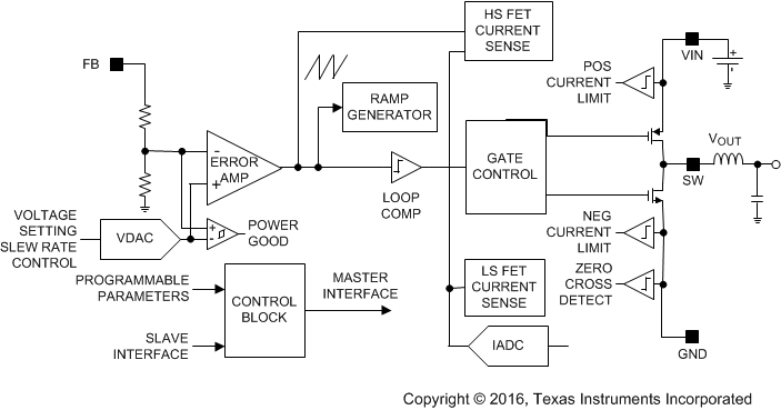
A block diagram of a single core is shown in Figure 7-1.
 Figure 7-1 Detailed Block Diagram Showing One Core