SNVSB64A June 2019 – June 2021 LP8733-Q1
PRODUCTION DATA
- 1 Features
- 2 Applications
- 3 Description
- 4 Revision History
- 5 Pin Configuration and Functions
- 6 Specifications
-
7 Detailed Description
- 7.1 Overview
- 7.2 Functional Block Diagram
- 7.3
Feature Description
- 7.3.1 DC/DC Converters
- 7.3.2 Sync Clock Functionality
- 7.3.3 Low-Dropout Linear Regulators (LDOs)
- 7.3.4 Power-Up
- 7.3.5 Regulator Control
- 7.3.6 Enable and Disable Sequences
- 7.3.7 Device Reset Scenarios
- 7.3.8 Diagnosis and Protection Features
- 7.3.9 Operation of the GPO Signals
- 7.3.10 Digital Signal Filtering
- 7.4 Device Functional Modes
- 7.5 Programming
- 7.6
Register Maps
- 7.6.1
Register Descriptions
- 7.6.1.1 DEV_REV
- 7.6.1.2 OTP_REV
- 7.6.1.3 BUCK0_CTRL_1
- 7.6.1.4 BUCK0_CTRL_2
- 7.6.1.5 BUCK1_CTRL_1
- 7.6.1.6 BUCK1_CTRL_2
- 7.6.1.7 BUCK0_VOUT
- 7.6.1.8 BUCK1_VOUT
- 7.6.1.9 LDO0_CTRL
- 7.6.1.10 LDO1_CTRL
- 7.6.1.11 LDO0_VOUT
- 7.6.1.12 LDO1_VOUT
- 7.6.1.13 BUCK0_DELAY
- 7.6.1.14 BUCK1_DELAY
- 7.6.1.15 LDO0_DELAY
- 7.6.1.16 LDO1_DELAY
- 7.6.1.17 GPO_DELAY
- 7.6.1.18 GPO2_DELAY
- 7.6.1.19 GPO_CTRL
- 7.6.1.20 CONFIG
- 7.6.1.21 PLL_CTRL
- 7.6.1.22 PGOOD_CTRL_1
- 7.6.1.23 PGOOD_CTRL_2
- 7.6.1.24 PG_FAULT
- 7.6.1.25 RESET
- 7.6.1.26 INT_TOP_1
- 7.6.1.27 INT_TOP_2
- 7.6.1.28 INT_BUCK
- 7.6.1.29 INT_LDO
- 7.6.1.30 TOP_STAT
- 7.6.1.31 BUCK_STAT
- 7.6.1.32 LDO_STAT
- 7.6.1.33 TOP_MASK_1
- 7.6.1.34 TOP_MASK_2
- 7.6.1.35 BUCK_MASK
- 7.6.1.36 LDO_MASK
- 7.6.1.37 SEL_I_LOAD
- 7.6.1.38 I_LOAD_2
- 7.6.1.39 I_LOAD_1
- 7.6.1
Register Descriptions
- 8 Application and Implementation
- 9 Power Supply Recommendations
- 10Layout
- 11Device and Documentation Support
- 12Mechanical, Packaging, and Orderable Information
Package Options
Mechanical Data (Package|Pins)
- RHD|28
Thermal pad, mechanical data (Package|Pins)
- RHD|28
Orderable Information
7.3.5.2 Changing Output Voltage
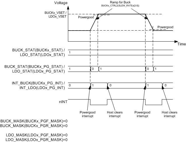
The output voltage of the regulator can be changed by writing to the BUCKx_VOUT and LDOx_VOUT register. The voltage change for the buck regulator is always slew-rate controlled, and the slew-rate is defined by the BUCKx_SLEW_RATE[2:0] bits in the BUCKx_CTRL_2 register. During voltage change, the forced PWM mode is used automatically. If the dual-phase operation is forced by the BUCK0_FPWM_MP bit in the BUCK0_CTRL_1 register, the regulator operates in dual-phase mode. If the dual-phase operation is not forced, the number of phases are added and shedded automatically to follow the required slew rate. When the programmed output voltage is achieved, the mode becomes the one defined by the load current, the BUCKx_FPWM bit in the BUCKx_CTRL_1 register, and the BUCK0_FPWM_MP bit.
The voltage change and Power-Good interrupts are shown in Figure 7-8.
 Figure 7-8 Regulator Output Voltage Change
During an LDO voltage change, the internal reference for the Power-Good detection is also changed. For this reason when the output voltage is changing, toggling of the Power-Good signal may still indicate a valid output. This period takes less than 100 µs and after that time the Power-Good gives correct value.