SNVSB23 March   2018 LP87521-Q1 , LP87522-Q1 , LP87523-Q1 , LP87524-Q1 , LP87525-Q1

PRODUCTION DATA.  

  1. Features
  2. Applications
    1.     Simplified Schematic
  3. Description
    1.     Efficiency vs Output Current
  4. Revision History
  5. Device Comparison Table
  6. Pin Configuration and Functions
    1.     Pin Functions
  7. Specifications
    1. 7.1 Absolute Maximum Ratings
    2. 7.2 ESD Ratings
    3. 7.3 Recommended Operating Conditions
    4. 7.4 Thermal Information
    5. 7.5 Electrical Characteristics
    6. 7.6 I2C Serial Bus Timing Requirements
    7. 7.7 Typical Characteristics
  8. Detailed Description
    1. 8.1 Overview
    2. 8.2 Functional Block Diagram
    3. 8.3 Feature Descriptions
      1. 8.3.1 Multi-Phase DC/DC Converters
        1. 8.3.1.1 Overview
        2. 8.3.1.2 Multiphase Operation, Phase Adding, and Phase-Shedding
        3. 8.3.1.3 Transition Between PWM and PFM Modes
        4. 8.3.1.4 Multiphase Switcher Configurations
        5. 8.3.1.5 Buck Converter Load-Current Measurement
        6. 8.3.1.6 Spread-Spectrum Mode
      2. 8.3.2 Sync Clock Functionality
      3. 8.3.3 Power-Up
      4. 8.3.4 Regulator Control
        1. 8.3.4.1 Enabling and Disabling Regulators
        2. 8.3.4.2 Changing Output Voltage
      5. 8.3.5 Enable and Disable Sequences
      6. 8.3.6 Device Reset Scenarios
      7. 8.3.7 Diagnosis and Protection Features
        1. 8.3.7.1 Power-Good Information (PGOOD Pin)
        2. 8.3.7.2 Warnings for Diagnosis (Interrupt)
          1. 8.3.7.2.1 Output Power Limit
          2. 8.3.7.2.2 Thermal Warning
        3. 8.3.7.3 Protection (Regulator Disable)
          1. 8.3.7.3.1 Short-Circuit and Overload Protection
          2. 8.3.7.3.2 Overvoltage Protection
          3. 8.3.7.3.3 Thermal Shutdown
        4. 8.3.7.4 Fault (Power Down)
          1. 8.3.7.4.1 Undervoltage Lockout
      8. 8.3.8 GPIO Signal Operation
      9. 8.3.9 Digital Signal Filtering
    4. 8.4 Device Functional Modes
      1. 8.4.1 Modes of Operation
    5. 8.5 Programming
      1. 8.5.1 I2C-Compatible Interface
        1. 8.5.1.1 Data Validity
        2. 8.5.1.2 Start and Stop Conditions
        3. 8.5.1.3 Transferring Data
        4. 8.5.1.4 I2C-Compatible Chip Address
        5. 8.5.1.5 Auto-Increment Feature
    6. 8.6 Register Maps
      1. 8.6.1 Register Descriptions
        1. 8.6.1.1  OTP_REV
        2. 8.6.1.2  BUCK0_CTRL1
        3. 8.6.1.3  BUCK1_CTRL1
        4. 8.6.1.4  BUCK2_CTRL1
        5. 8.6.1.5  BUCK3_CTRL1
        6. 8.6.1.6  BUCK0_VOUT
        7. 8.6.1.7  BUCK0_FLOOR_VOUT
        8. 8.6.1.8  BUCK1_VOUT
        9. 8.6.1.9  BUCK1_FLOOR_VOUT
        10. 8.6.1.10 BUCK2_VOUT
        11. 8.6.1.11 BUCK2_FLOOR_VOUT
        12. 8.6.1.12 BUCK3_VOUT
        13. 8.6.1.13 BUCK3_FLOOR_VOUT
        14. 8.6.1.14 BUCK0_DELAY
        15. 8.6.1.15 BUCK1_DELAY
        16. 8.6.1.16 BUCK2_DELAY
        17. 8.6.1.17 BUCK3_DELAY
        18. 8.6.1.18 GPIO2_DELAY
        19. 8.6.1.19 GPIO3_DELAY
        20. 8.6.1.20 RESET
        21. 8.6.1.21 CONFIG
        22. 8.6.1.22 INT_TOP1
        23. 8.6.1.23 INT_TOP2
        24. 8.6.1.24 INT_BUCK_0_1
        25. 8.6.1.25 INT_BUCK_2_3
        26. 8.6.1.26 TOP_STAT
        27. 8.6.1.27 BUCK_0_1_STAT
        28. 8.6.1.28 BUCK_2_3_STAT
        29. 8.6.1.29 TOP_MASK1
        30. 8.6.1.30 TOP_MASK2
        31. 8.6.1.31 BUCK_0_1_MASK
        32. 8.6.1.32 BUCK_2_3_MASK
        33. 8.6.1.33 SEL_I_LOAD
        34. 8.6.1.34 I_LOAD_2
        35. 8.6.1.35 I_LOAD_1
        36. 8.6.1.36 PGOOD_CTRL1
        37. 8.6.1.37 PGOOD_CTRL2
        38. 8.6.1.38 PGOOD_FLT
        39. 8.6.1.39 PLL_CTRL
        40. 8.6.1.40 PIN_FUNCTION
        41. 8.6.1.41 GPIO_CONFIG
        42. 8.6.1.42 GPIO_IN
        43. 8.6.1.43 GPIO_OUT
  9. Application and Implementation
    1. 9.1 Application Information
    2. 9.2 Typical Applications
      1. 9.2.1 Design Requirements
        1. 9.2.1.1 Inductor Selection
        2. 9.2.1.2 Input Capacitor Selection
        3. 9.2.1.3 Output Capacitor Selection
        4. 9.2.1.4 Snubber Components
        5. 9.2.1.5 Supply Filtering Components
        6. 9.2.1.6 Current Limit vs. Maximum Output Current
      2. 9.2.2 Detailed Design Procedure
      3. 9.2.3 Application Curves
  10. 10Power Supply Recommendations
  11. 11Layout
    1. 11.1 Layout Guidelines
    2. 11.2 Layout Example
  12. 12Device and Documentation Support
    1. 12.1 Device Support
      1. 12.1.1 Third-Party Products Disclaimer
    2. 12.2 Documentation Support
      1. 12.2.1 Related Documentation
    3. 12.3 Related Links
    4. 12.4 Receiving Notification of Documentation Updates
    5. 12.5 Community Resources
    6. 12.6 Trademarks
    7. 12.7 Electrostatic Discharge Caution
    8. 12.8 Glossary
  13. 13Mechanical, Packaging, and Orderable Information

Package Options

Refer to the PDF data sheet for device specific package drawings

Mechanical Data (Package|Pins)
  • RNF|26
Thermal pad, mechanical data (Package|Pins)
Orderable Information

Spread-Spectrum Mode

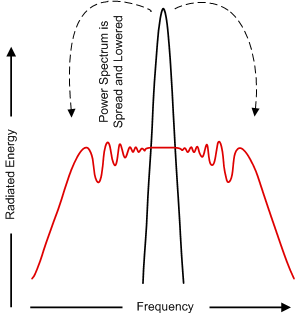
Systems with periodic switching signals may generate a large amount of switching noise in a set of narrowband frequencies (the switching frequency and its harmonics). The usual solution to decrease noise coupling is to add EMI filters and shields to the boards. The LP8752x-Q1 device has register-selectable spread-spectrum mode which minimizes the need for output filters, ferrite beads, or chokes. In spread-spectrum mode, the switching frequency varies around the center frequency, reducing the EMI emissions radiated by the converter and associated passive components and PCB traces (see Figure 12). This feature is available only when internal RC oscillator is used (PLL_MODE[1:0] = 00 in PLL_CTRL register), and it is enabled with the EN_SPREAD_SPEC bit (PIN_FUNCTION register), and it affects all the buck cores.
LP87521-Q1 LP87522-Q1 LP87523-Q1 LP87524-Q1 LP87525-Q1 30190611.gif
Where a fixed-frequency converter exhibits large amounts of spectral energy at the switching frequency, the spread-spectrum architecture of the LP8752x-Q1 spreads that energy over a large bandwidth.
Figure 12. Spread-Spectrum Modulation