SNVSBA3 December 2020 LP875761-Q1
PRODUCTION DATA
- 1 Features
- 2 Applications
- 3 Description
- 4 Revision History
- 5 Pin Configuration and Functions
- 6 Specifications
-
7 Detailed Description
- 7.1 Overview
- 7.2 Functional Block Diagram
- 7.3
Feature Descriptions
- 7.3.1 Multi-Phase DC/DC Converters
- 7.3.2 Sync Clock Functionality
- 7.3.3 Power-Up
- 7.3.4 Regulator Control
- 7.3.5 Enable and Disable Sequences
- 7.3.6 Device Reset Scenarios
- 7.3.7 Diagnosis and Protection Features
- 7.3.8 GPIO Signal Operation
- 7.3.9 Digital Signal Filtering
- 7.4 Device Functional Modes
- 7.5 Programming
- 7.6
Register Maps
- 7.6.1
Register Descriptions
- 53
- 7.6.1.1 DEV_REV
- 7.6.1.2 OTP_REV
- 7.6.1.3 BUCK0_CTRL1
- 7.6.1.4 BUCK0_CTRL2
- 7.6.1.5 BUCK1_CTRL2
- 7.6.1.6 BUCK2_CTRL2
- 7.6.1.7 BUCK3_CTRL2
- 7.6.1.8 BUCK0_DELAY
- 7.6.1.9 GPIO2_DELAY
- 7.6.1.10 GPIO3_DELAY
- 7.6.1.11 RESET
- 7.6.1.12 CONFIG
- 7.6.1.13 INT_TOP1
- 7.6.1.14 INT_TOP2
- 7.6.1.15 INT_BUCK_0_1
- 7.6.1.16 INT_BUCK_2_3
- 7.6.1.17 TOP_STAT
- 7.6.1.18 BUCK_0_1_STAT
- 7.6.1.19 BUCK_2_3_STAT
- 7.6.1.20 TOP_MASK1
- 7.6.1.21 TOP_MASK2
- 7.6.1.22 BUCK_0_1_MASK
- 7.6.1.23 BUCK_2_3_MASK
- 7.6.1.24 SEL_I_LOAD
- 7.6.1.25 I_LOAD_2
- 7.6.1.26 I_LOAD_1
- 7.6.1.27 PGOOD_CTRL1
- 7.6.1.28 PGOOD_CTRL2
- 7.6.1.29 PGOOD_FLT
- 7.6.1.30 PLL_CTRL
- 7.6.1.31 PIN_FUNCTION
- 7.6.1.32 GPIO_CONFIG
- 7.6.1.33 GPIO_IN
- 7.6.1.34 GPIO_OUT
- 7.6.1
Register Descriptions
- 8 Application and Implementation
- 9 Power Supply Recommendations
- 10Layout
- 11Device and Documentation Support
- 12Mechanical, Packaging, and Orderable Information
Package Options
Refer to the PDF data sheet for device specific package drawings
Mechanical Data (Package|Pins)
- RNF|26
Thermal pad, mechanical data (Package|Pins)
Orderable Information
7.3.1.1 Overview
The LP875761-Q1 includes four step-down DC/DC converter cores which are configured as a 4-phase single output.
TheLP875761-Q1 has the following features:
- Optional external clock input to minimize crosstalk
- Optional spread spectrum technique to decrease EMI
- Phase control for optimized EMI
- Synchronous rectification
- Current mode loop with PI compensator
- Soft start
- Power Good flag with maskable interrupt
- Power Good signal (PGOOD) with selectable sources
- Average output current sensing (for load current measurement)
- Current balancing between the phases of the converter
- Differential voltage sensing from point of the load for multiphase output
The following parameters can be programmed via registers:
- Forced multiphase operation for multiphase outputs (forces also the PWM operation)
- Peak current limit for high-side FET
- Enable and disable delays for regulators and GPIOs controlled by ENx pins
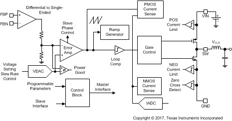
The 4 buck converters in the LP875761-Q1 operate in forced multiphase configuration as one 4-phase converter, which offers several advantages over one power stage converter. For application processor power delivery, lower ripple on the input and output currents and faster transient response to load steps are the most significant advantages. Also, because the load current is evenly shared among multiple channels in multiphase output configuration, the heat generated is greatly decreased for each channel due to the fact that power loss is proportional to square of current. The physical size of the output inductor shrinks significantly due to this heat reduction. Figure 7-1 shows a block diagram of a single core.
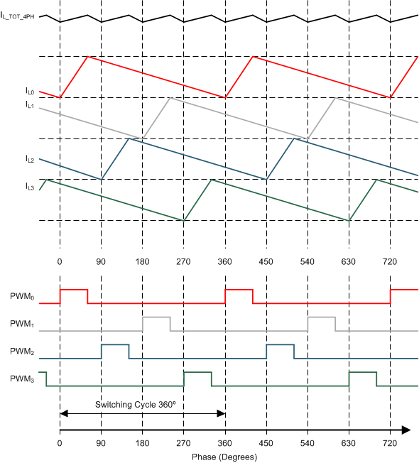
Interleaving switching action of the 4-phase converter is shown in Figure 7-2. The 4-phase converter switches each channel 90° apart. As a result, the 4-phase converter has an effective ripple frequency four times greater than the switching frequency of a one phase converter
 Figure 7-1 Detailed Block Diagram Showing One Core