Measurements are done using typical application set up with connections shown in Figure 8-1. Graphs may not reflect the OTP default settings. Unless otherwise specified: VIN = 3.7 V, V(NRST) = 1.8 V, TA = 25 °C, ƒSW = 3 MHz, L = 470 nH (TDK VLS252010HBX-R47M), ILIM FWD set to maximum 5 A.

| VIN = 3.7 V | |
| VOUT settings = 1000 mV, 1200 mV, 1800 mV, and 2500 mV |

| Load = 1A | |
| VOUT settings = 1000 mV, 1200 mV, 1800 mV, and 2500 mV |

| Change in Output Voltage from Zero Load (%) | |
| VOUT settings = 1000 mV, 1200 mV, 1800 mV, and 2500 mV |
 Figure 8-8 Output Voltage vs Load Current in PWM-PFM Mode
| VOUT setting = 1000 mV | |
| Load = 1 A (PWM Mode) and 100 mA (PFM Mode) |
 Figure 8-12 Start-up with EN1
| Load = 0 A | Enable and disable delays = default |
| VOUT settings = default | |
 Figure 8-16 Output Voltage Ripple, PFM Mode
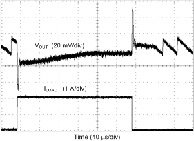
 Figure 8-18 Transient from PFM-to-PWM Mode
| Load = 4 A | VOUT = 1000 mV |
| VIN stepping 3.3 V ↔ 3.8 V, TR = TF = 10 µs |

| Load = 0 A → 2 A → 0 A | TR = TF = 400 ns | VOUT = 1 V |
| | |
 Figure 8-24 VOUT Transition From 0.6 V to 1.4 V With Different Slew Rate Settings
| Load = 100 mA | |
| VOUT settings = 1000 mV, 1200 mV, 1800 mV, and 2500 mV |

| Load = 3A | | |
| VOUT settings = 1000 mV, 1200 mV, 1800 mV, and 2500 mV |
 Figure 8-7 Output Voltage vs Load Current in PWM-PFM Mode
| Change in Output Voltage from VIN = 3.7 V (%) | Load = 1 A |
| VOUT settings = 1000 mV, 1200 mV, 1800 mV, and 2500 mV |
 Figure 8-11 Start-up with EN1
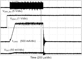
 Figure 8-13 Start-up With Short on Output
 Figure 8-15 Shutdown with EN1
 Figure 8-17 Output Voltage Ripple, Forced PWM Mode
 Figure 8-19 Transient from PWM-to-PFM Mode
| Load = 0 A → 2 A → 0 A | TR = TF = 400 ns | VOUT = 1 V |
| | |

| Load = 1A → 4 A → 1A | TR = TF = 1 µs | VOUT = 1 V |
| | |
 Figure 8-25 VOUT Transition From 1.4 V to 0.6 V With Different Slew Rate Settings


 Figure 8-18 Transient from PFM-to-PWM Mode

 Figure 8-24 VOUT Transition From 0.6 V to 1.4 V With Different Slew Rate Settings


 Figure 8-13 Start-up With Short on Output

 Figure 8-19 Transient from PWM-to-PFM Mode

 Figure 8-25 VOUT Transition From 1.4 V to 0.6 V With Different Slew Rate Settings