-
LP8769-Q1 High Frequency Quad Step-Down DC-DC
Package Options
Mechanical Data (Package|Pins)
- RQK|32
Thermal pad, mechanical data (Package|Pins)
Orderable Information
LP8769-Q1 High Frequency Quad Step-Down DC-DC
1 Features
- AEC-Q100 Qualified with the
following results:
- Input voltage: 2.8 V to 5.5 V
- Device temperature grade 1: –40°C to +125°C ambient operating temperature range
- Device HBM ESD classification Level 2
- Device CDM ESD classification Level C4B
- Functional Safety-Compliant
- Developed for functional safety applications
- Documentation available to aid ISO 26262 system design up to ASIL-D
- Documentation available to aid IEC 61508 system design up to SIL-3
- Systematic capability up to ASIL-D
- Hardware integrity up to ASIL-D
- Windowed voltage and over-current monitors
- Watchdog with selectable trigger / Q&A mode
- Level or PWM error signal monitoring (ESM)
- Thermal monitoring with high temperature warning and thermal shutdown
- Bit-integrity (CRC) error detection on configuration registers and non-volatile memory
- 4 high-efficiency step-down DC/DC
converters:
- Output voltage: 0.3 V to 3.34 V (0.3 V to 1.9 V for multi-phase outputs)
- Maximum output current: 5 A per phase, up to 20 A with 4-phase configuration
- Programmable output voltage slew-rate: 0.5 mV/µs to 33 mV/µs
- Switching frequency: 2.2 MHz or 4.4 MHz
- 10 configurable general purpose I/O (GPIO)
- SPMI interface for multi-PMIC synchronization
- Input overvoltage monitor (OVP) and undervoltage lockout (UVLO)
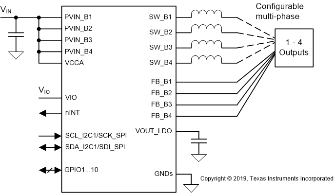
 Simplified Schematic
3 Description
The LP8769x-Q1 device is designed to meet the power management requirements of the latest processors and platforms in various safety-relevant automotive and industrial applications. The device has four step-down DC/DC converter cores, that are configurable for five different phase configurations from one 4-phase output to four 1-phase outputs. The device settings can be changed by I2C-compatible serial interface or by a SPI serial interface.
The automatic PFM/PWM (AUTO mode) operation together with the automatic phase adding and phase shedding maximizes efficiency over a wide output-current range. The LP8769x-Q1 device supports remote differential voltage sensing for multiphase outputs to compensate IR drop between the regulator output and the point-of-load (POL) that improves the accuracy of the output voltage. The switching clock can be forced to PWM mode and the phases are interleaved. The switching can be synchronized to an external clock and spread-spectrum mode can be enabled to minimize the disturbances.
| PART NUMBER | PACKAGE | BODY SIZE (NOM) |
|---|---|---|
| LP8769-Q1 | VQFN-HR (32) | 5.50 mm × 5.00 mm |