SNVSAL1C December 2017 – June 2021 LP87702-Q1
PRODUCTION DATA
- 1 Features
- 2 Applications
- 3 Description
- 4 Revision History
- 5 Description (continued)
- 6 Pin Configuration and Functions
- 7 Specifications
-
8 Detailed Description
- 8.1 Overview
- 8.2 Functional Block Diagram
- 8.3
Feature Descriptions
- 8.3.1 Step-Down DC/DC Converters
- 8.3.2 Boost Converter
- 8.3.3 Spread-Spectrum Mode
- 8.3.4 Sync Clock Functionality
- 8.3.5 Power-Up
- 8.3.6 Buck and Boost Control
- 8.3.7 Enable and Disable Sequences
- 8.3.8 Window Watchdog
- 8.3.9 Device Reset Scenarios
- 8.3.10 Diagnostics and Protection Features
- 8.3.11 OTP Error Correction
- 8.3.12 Operation of GPO Signals
- 8.3.13 Digital Signal Filtering
- 8.4 Device Functional Modes
- 8.5 Programming
- 8.6 Register Maps
- 9 Application and Implementation
- 10Power Supply Recommendations
- 11Layout
- 12Device and Documentation Support
- 13Mechanical, Packaging, and Orderable Information
Package Options
Mechanical Data (Package|Pins)
- RHB|32
Thermal pad, mechanical data (Package|Pins)
- RHB|32
Orderable Information
6 Pin Configuration and Functions
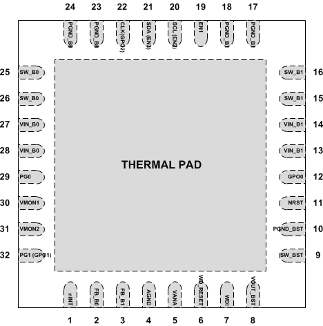
 Figure 6-1 RHB Package32-Pin VQFN With Thermal PadTop View
Table 6-1 Pin Functions
| PIN | TYPE | DESCRIPTION | |
|---|---|---|---|
| NAME | NUMBER | ||
| AGND | 4 | G | Ground |
| CLKIN | 22 | D/I/O | External clock input. Alternative function is general purpose digital output 2 (GPO2). Second alternative function is watchdog disable (WD_DIS) |
| EN1 | 19 | D/I | Programmable Enable 1 signal. |
| FB_B0 | 2 | A | Output voltage feedback for Buck0. |
| FB_B1 | 3 | A | Output voltage feedback for Buck1. |
| GPO0 | 12 | D/O | General purpose digital output 0. |
| nINT | 1 | D/O | Open-drain interrupt output. Active LOW. |
| NRST | 11 | D/I | Reset signal for the device. |
| PG0 | 29 | D/O | Programmable power-good indication signal. |
| PG1 | 32 | D/O | Programmable power-good indication signal. Alternative function is general purpose digital output 1 (GPO1). |
| PGND_B0 | 23, 24 | P/G | Power ground for Buck0. |
| PGND_B1 | 17, 18 | P/G | Power Ground for Buck1. |
| PGND_BST | 10 | P/G | Power ground for boost. |
| SCL | 20 | D/I | Serial interface clock input for I2C access. Connect a pullup resistor. Alternative function is programmable to the enable 2 signal. |
| SDA | 21 | D/I/O | Serial interface data input and output for I2C access. Connect a pullup resistor. Alternative function is programmable to the enable 3 signal. |
| SW_B0 | 25, 26 | P/O | Buck0 switch node. |
| SW_B1 | 15, 16 | P/O | Buck1 switch node. |
| SW_BST | 9 | P/I | Boost input. Bypass switch input when this mode is selected. |
| VANA | 5 | P | Supply voltage for analog and digital blocks. Must be connected to same node with VIN_Bx. |
| VMON1 | 30 | A/I | Voltage monitoring input 1. |
| VMON2 | 31 | A/I | Voltage monitoring input 2. |
| VIN_B0 | 27, 28 | P/I | Input for Buck0. The separate power pins VIN_Bx are not connected together internally – VIN_Bx pins must be connected together in the application and be locally bypassed. |
| VIN_B1 | 13, 14 | P/I | Input for Buck1. The separate power pins VIN_Bx are not connected together internally – VIN_Bx pins must be connected together in the application and be locally bypassed. |
| VOUT_BST | 8 | P/O | Boost output. Bypass switch output when this mode is selected. |
| WD_RESET | 6 | D/O | Reset output from window watchdog |
| WDI | 7 | D/I | Digital input signal for window watchdog |
| Thermal pad | N/A | G | |
| A: Analog Pin, D: Digital Pin, G: Ground Pin, P: Power Pin, I: Input Pin, O: Output Pin | |||