SNVSAL1C December   2017  – June 2021 LP87702-Q1

PRODUCTION DATA  

  1. Features
  2. Applications
  3. Description
  4. Revision History
  5. Description (continued)
  6. Pin Configuration and Functions
  7. Specifications
    1. 7.1 Absolute Maximum Ratings
    2. 7.2 ESD Ratings
    3. 7.3 Recommended Operating Conditions
    4. 7.4 Thermal Information
    5. 7.5 Electrical Characteristics
    6. 7.6 I2C Serial Bus Timing Parameters
    7. 7.7 Typical Characteristics
  8. Detailed Description
    1. 8.1 Overview
    2. 8.2 Functional Block Diagram
    3. 8.3 Feature Descriptions
      1. 8.3.1  Step-Down DC/DC Converters
        1. 8.3.1.1 Overview
        2. 8.3.1.2 Transition Between PWM and PFM Modes
        3. 8.3.1.3 Buck Converter Load Current Measurement
      2. 8.3.2  Boost Converter
      3. 8.3.3  Spread-Spectrum Mode
      4. 8.3.4  Sync Clock Functionality
      5. 8.3.5  Power-Up
      6. 8.3.6  Buck and Boost Control
        1. 8.3.6.1 Enabling and Disabling Converters
        2. 8.3.6.2 Changing Buck Output Voltage
      7. 8.3.7  Enable and Disable Sequences
      8. 8.3.8  Window Watchdog
      9. 8.3.9  Device Reset Scenarios
      10. 8.3.10 Diagnostics and Protection Features
        1. 8.3.10.1 Voltage Monitorings
        2. 8.3.10.2 Interrupts
        3. 8.3.10.3 Power-Good Information to Interrupt, PG0, and PG1 Pins
          1. 8.3.10.3.1 PGx Pin Gated (Unusual) Mode
          2. 8.3.10.3.2 PGx Pin Operation in Continuous Mode
          3. 8.3.10.3.3 Summary of PG0, PG1 Gated, and Continuous Operating Modes
        4. 8.3.10.4 Warning Interrupts for System Level Diagnostics
          1. 8.3.10.4.1 Output Power Limit
          2. 8.3.10.4.2 Thermal Warning
        5. 8.3.10.5 Protections Causing Converter Disable
          1. 8.3.10.5.1 Short-Circuit and Overload Protection
          2. 8.3.10.5.2 Overvoltage Protection
          3. 8.3.10.5.3 Thermal Shutdown
        6. 8.3.10.6 Protections Causing Device Power Down
          1. 8.3.10.6.1 Undervoltage Lockout
      11. 8.3.11 OTP Error Correction
      12. 8.3.12 Operation of GPO Signals
      13. 8.3.13 Digital Signal Filtering
    4. 8.4 Device Functional Modes
      1. 8.4.1 Modes of Operation
    5. 8.5 Programming
      1. 8.5.1 I2C-Compatible Interface
        1. 8.5.1.1 Data Validity
        2. 8.5.1.2 Start and Stop Conditions
        3. 8.5.1.3 Transferring Data
        4. 8.5.1.4 I2C-Compatible Chip Address
        5. 8.5.1.5 Auto Increment Feature
    6. 8.6 Register Maps
      1. 8.6.1 Register Descriptions
        1. 8.6.1.1 LP8770_map Registers
  9. Application and Implementation
    1. 9.1 Application Information
    2. 9.2 Typical Application
      1. 9.2.1 Design Requirements
      2. 9.2.2 Detailed Design Procedure
        1. 9.2.2.1 Application Components
          1. 9.2.2.1.1 Inductor Selection
          2. 9.2.2.1.2 Buck Input Capacitor Selection
          3. 9.2.2.1.3 Buck Output Capacitor Selection
          4. 9.2.2.1.4 Boost Input Capacitor Selection
          5. 9.2.2.1.5 Boost Output Capacitor Selection
          6. 9.2.2.1.6 Supply Filtering Components
      3. 9.2.3 Current Limit vs Maximum Output Current
      4. 9.2.4 Application Curves
  10. 10Power Supply Recommendations
  11. 11Layout
    1. 11.1 Layout Guidelines
    2. 11.2 Layout Example
  12. 12Device and Documentation Support
    1. 12.1 Third-Party Products Disclaimer
    2. 12.2 Receiving Notification of Documentation Updates
    3. 12.3 Support Resources
    4. 12.4 Trademarks
    5. 12.5 Electrostatic Discharge Caution
    6. 12.6 Glossary
  13. 13Mechanical, Packaging, and Orderable Information

Package Options

Mechanical Data (Package|Pins)
Thermal pad, mechanical data (Package|Pins)
Orderable Information

Spread-Spectrum Mode

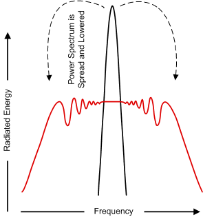
Systems with periodic switching signals may generate a large amount of switching noise in a set of narrowband frequencies (the switching frequency and its harmonics). The usual solution to reduce noise coupling is to add EMI-filters and shields to the boards. The LP87702-Q1 device supports the spread-spectrum switching frequency modulation mode that is register controlled. This mode minimizes the need for output filters, ferrite beads, or chokes. The switching frequency varies between 0.85 × fSW and fSW in spread spectrum mode, where fSW is switching the frequency selected in the OTP. Figure 8-2 shows how the spread spectrum modulation reduces conducted and radiated emissions by the converter and associated passive components and PCB traces. This feature is available only when internal RC oscillator is used (EN_PLL is 0 in PLL_CTRL register) and it is enabled with the EN_SPREAD_SPEC bit in CONFIG register, and it affects both buck converters and the boost converter.
GUID-6F0D0821-DAC6-409D-B3F0-11701FF216A7-low.gif
Where a fixed frequency converter exhibits large amounts of spectral energy at the switching frequency, the spread spectrum architecture of the LP87702-Q1 spreads that energy over a large bandwidth.
Figure 8-2 Spread Spectrum Modulation