SNVSBU3 March   2021 LP87702

PRODUCTION DATA  

  1. Features
  2. Applications
  3. Description
  4. Revision History
  5. Pin Configuration and Functions
  6. Specifications
    1. 6.1 Absolute Maximum Ratings
    2. 6.2 ESD Ratings
    3. 6.3 Recommended Operating Conditions
    4. 6.4 Thermal Information
    5. 6.5 Electrical Characteristics
    6. 6.6 I2C Serial Bus Timing Parameters
    7. 6.7 Typical Characteristics
  7. Detailed Description
    1. 7.1 Overview
    2. 7.2 Functional Block Diagram
    3. 7.3 Feature Descriptions
      1. 7.3.1  Step-Down DC/DC Converters
        1. 7.3.1.1 Overview
        2. 7.3.1.2 Transition Between PWM and PFM Modes
        3. 7.3.1.3 Buck Converter Load Current Measurement
      2. 7.3.2  Boost Converter
      3. 7.3.3  Spread-Spectrum Mode
      4. 7.3.4  Sync Clock Functionality
      5. 7.3.5  Power-Up
      6. 7.3.6  Buck and Boost Control
        1. 7.3.6.1 Enabling and Disabling Converters
        2. 7.3.6.2 Changing Buck Output Voltage
      7. 7.3.7  Enable and Disable Sequences
      8. 7.3.8  Window Watchdog
      9. 7.3.9  Device Reset Scenarios
      10. 7.3.10 Diagnostics and Protection Features
        1. 7.3.10.1 Voltage Monitorings
        2. 7.3.10.2 Interrupts
        3. 7.3.10.3 Power-Good Information to Interrupt, PG0, and PG1 Pins
          1. 7.3.10.3.1 PGx Pin Gated (Unusual) Mode
          2. 7.3.10.3.2 PGx Pin Operation in Continuous Mode
          3. 7.3.10.3.3 Summary of PG0, PG1 Gated, and Continuous Operating Modes
        4. 7.3.10.4 Warning Interrupts for System Level Diagnostics
          1. 7.3.10.4.1 Output Power Limit
          2. 7.3.10.4.2 Thermal Warning
        5. 7.3.10.5 Protections Causing Converter Disable
          1. 7.3.10.5.1 Short-Circuit and Overload Protection
          2. 7.3.10.5.2 Overvoltage Protection
          3. 7.3.10.5.3 Thermal Shutdown
        6. 7.3.10.6 Protections Causing Device Power Down
          1. 7.3.10.6.1 Undervoltage Lockout
      11. 7.3.11 OTP Error Correction
      12. 7.3.12 Operation of GPO Signals
      13. 7.3.13 Digital Signal Filtering
    4. 7.4 Device Functional Modes
      1. 7.4.1 Modes of Operation
    5. 7.5 Programming
      1. 7.5.1 I2C-Compatible Interface
        1. 7.5.1.1 Data Validity
        2. 7.5.1.2 Start and Stop Conditions
        3. 7.5.1.3 Transferring Data
        4. 7.5.1.4 I2C-Compatible Chip Address
        5. 7.5.1.5 Auto Increment Feature
    6. 7.6 Register Maps
      1. 7.6.1 Register Descriptions
        1. 7.6.1.1 LP8770_map Registers
  8. Application and Implementation
    1. 8.1 Application Information
    2. 8.2 Typical Application
      1. 8.2.1 Design Requirements
      2. 8.2.2 Detailed Design Procedure
        1. 8.2.2.1 Application Components
          1. 8.2.2.1.1 Inductor Selection
          2. 8.2.2.1.2 Buck Input Capacitor Selection
          3. 8.2.2.1.3 Buck Output Capacitor Selection
          4. 8.2.2.1.4 Boost Input Capacitor Selection
          5. 8.2.2.1.5 Boost Output Capacitor Selection
          6. 8.2.2.1.6 Supply Filtering Components
      3. 8.2.3 Current Limit vs Maximum Output Current
      4. 8.2.4 Application Curves
  9. Power Supply Recommendations
  10. 10Layout
    1. 10.1 Layout Guidelines
    2. 10.2 Layout Example
  11. 11Device and Documentation Support
    1. 11.1 Third-Party Products Disclaimer
    2. 11.2 Receiving Notification of Documentation Updates
    3. 11.3 Support Resources
    4. 11.4 Trademarks
    5. 11.5 Electrostatic Discharge Caution
    6. 11.6 Glossary
  12. 12Mechanical, Packaging, and Orderable Information

Package Options

Mechanical Data (Package|Pins)
Thermal pad, mechanical data (Package|Pins)
Orderable Information

Current Limit vs Maximum Output Current

The current limit must be set high enough to account for the inductor ripple current on top of the maximum output current for the buck converters and boost. The forward current limit for the buck converters is set by BUCK0_ILIM, BUCK1_ILIM and for boost it is set by BOOST_ILIM.

For the buck converter the inductor current ripple can be calculated using Equation 1 and Equation 2:

Equation 1. GUID-68ADD749-A77C-442C-BD0A-19DE6222118C-low.gif
Equation 2. GUID-A1661C10-3BDB-4B4A-95AB-0076DD8DAAE9-low.gif

Example using Equation 1 and Equation 2:

VIN(max) = 5.5 V
VOUT = 1 V
η = 0.75
fSW = 1.8 MHz
L = 0.38 µH
then D = 0.242 and ΔIL = 1.59 A

Peak current is half of the current ripple. If ILIM_FWD_SET_OTP is 3 A, the minimum forward current limit would be 2.85 A when taking the –5% tolerance into account. In this case the difference between set peak current and maximum load current = 0.795 A + 0.15 A = 0.945 A.
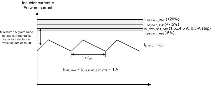
GUID-F521B70B-CEE8-412C-8753-2280D0651DB5-low.gifFigure 8-2 Current Limit vs Maximum Output Current