SNVSA21G May 2014 – October 2017 LP8860-Q1
PRODUCTION DATA.
- 1 Features
- 2 Applications
- 3 Description
- 4 Revision History
- 5 Device Comparison Table
- 6 Pin Configuration and Functions
-
7 Specifications
- 7.1 Absolute Maximum Ratings
- 7.2 ESD Ratings
- 7.3 Recommended Operating Conditions
- 7.4 Thermal Information
- 7.5 Electrical Characteristics
- 7.6 Current Sinks Electrical Characteristics
- 7.7 Boost Converter Characteristics
- 7.8 Logic Interface Characteristics
- 7.9 VIN Undervoltage Protection (VIN_UVLO)
- 7.10 VDD Undervoltage Protection (VDD_UVLO)
- 7.11 VIN Overvoltage Protection (VIN_OVP)
- 7.12 VIN Overcurrent Protection (VIN_OCP)
- 7.13 Power-Line FET Control Electrical Characteristics
- 7.14 External Temp Sensor Control Electrical Characteristics
- 7.15 I2C Serial Bus Timing Parameters (SDA, SCLK)
- 7.16 SPI Timing Requirements
- 7.17 Typical Characteristics
-
8 Detailed Description
- 8.1 Overview
- 8.2 Functional Block Diagram
- 8.3 Feature Description
- 8.4 Device Functional Modes
- 8.5 Programming
- 8.6
Register Maps
- 8.6.1
Register Bit Explanations
- 8.6.1.1 Display/Cluster1 Brightness Control MSB
- 8.6.1.2 Display/Cluster1 Brightness Control LSB
- 8.6.1.3 Display/Cluster1 Output Current MSB
- 8.6.1.4 Display/Cluster1 Output Current LSB
- 8.6.1.5 Cluster2 Brightness Control MSB
- 8.6.1.6 Cluster2 Brightness Control LSB
- 8.6.1.7 Cluster2 Output Current
- 8.6.1.8 Cluster3 Brightness Control MSB
- 8.6.1.9 Cluster3 Brightness Control LSB
- 8.6.1.10 Cluster3 Output Current
- 8.6.1.11 Cluster4 Brightness Control MSB
- 8.6.1.12 Cluster4 Brightness Control LSB
- 8.6.1.13 Cluster4 Output Current
- 8.6.1.14 Configuration
- 8.6.1.15 Status
- 8.6.1.16 Fault
- 8.6.1.17 LED Fault
- 8.6.1.18 Fault Clear
- 8.6.1.19 Identification
- 8.6.1.20 Temp MSB
- 8.6.1.21 Temp LSB
- 8.6.1.22 Display LED Current MSB
- 8.6.1.23 Display LED Current LSB
- 8.6.1.24 Display LED PWM MSB
- 8.6.1.25 Display LED PWM LSB
- 8.6.1.26 EEPROM Control
- 8.6.1.27 EEPROM Unlock Code
- 8.6.2
EEPROM Bit Explanations
- 8.6.2.1 EEPROM Register 0
- 8.6.2.2 EEPROM Register 1
- 8.6.2.3 EEPROM Register 2
- 8.6.2.4 EEPROM Register 3
- 8.6.2.5 EEPROM Register 4
- 8.6.2.6 EEPROM Register 5
- 8.6.2.7 EEPROM Register 6
- 8.6.2.8 EEPROM Register 7
- 8.6.2.9 EEPROM Register 8
- 8.6.2.10 EEPROM Register 9
- 8.6.2.11 EEPROM Register 10
- 8.6.2.12 EEPROM Register 11
- 8.6.2.13 EEPROM Register 12
- 8.6.2.14 EEPROM Register 13
- 8.6.2.15 EEPROM Register 14
- 8.6.2.16 EEPROM Register 15
- 8.6.2.17 EEPROM Register 16
- 8.6.2.18 EEPROM Register 17
- 8.6.2.19 EEPROM Register 18
- 8.6.2.20 EEPROM Register 19
- 8.6.2.21 EEPROM Register 20
- 8.6.2.22 EEPROM Register 21
- 8.6.2.23 EEPROM Register 22
- 8.6.2.24 EEPROM Register 23
- 8.6.2.25 EEPROM Register 24
- 8.6.1
Register Bit Explanations
-
9 Application and Implementation
- 9.1 Application Information
- 9.2
Typical Applications
- 9.2.1
Typical Application for Display Backlight
- 9.2.1.1 Design Requirements
- 9.2.1.2
Detailed Design Procedure
- 9.2.1.2.1 Inductor Selection
- 9.2.1.2.2 Output Capacitor Selection
- 9.2.1.2.3 Input Capacitor Selection
- 9.2.1.2.4 Charge Pump Output Capacitor
- 9.2.1.2.5 Charge Pump Flying Capacitor
- 9.2.1.2.6 Diode
- 9.2.1.2.7 Boost Converter Transistor
- 9.2.1.2.8 Boost Sense Resistor
- 9.2.1.2.9 Power Line Transistor
- 9.2.1.2.10 Input Current Sense Resistor
- 9.2.1.2.11 Filter Component Values
- 9.2.1.3 Application Performance Plots
- 9.2.2 Low VDD Voltage and Combined Output Mode Application
- 9.2.3 High Output Voltage Application
- 9.2.4 High Output Current Application
- 9.2.5 Three-Channel Configuration Without Serial Interface
- 9.2.6 Solution With Minimum External Components
- 9.2.1
Typical Application for Display Backlight
- 10Power Supply Recommendations
- 11Layout
- 12Device and Documentation Support
- 13Mechanical, Packaging, and Orderable Information
Package Options
Mechanical Data (Package|Pins)
- VFP|32
Thermal pad, mechanical data (Package|Pins)
- VFP|32
Orderable Information
9 Application and Implementation
NOTE
Information in the following applications sections is not part of the TI component specification, and TI does not warrant its accuracy or completeness. TI’s customers are responsible for determining suitability of components for their purposes. Customers should validate and test their design implementation to confirm system functionality.
9.1 Application Information
The LP8860-Q1 is designed for automotive applications, and an input voltage VIN is intended to be connected to the car battery. The device is internally powered from the VDD pin, and voltage must be in 3-V to 5.5-V range. The device has flexible configurability; outputs configuration are defined by EEPROM settings. If the VDD voltage is not high enough to drive an external nMOSFET gate, an internal charge pump must be used to power the gate driver. The charge pump is configured by EEPROM.
The LP8860-Q1 can be used as a stand-alone device, using only the VDDIO/EN pin and the PWM signal. Alternatively, the device can be a part of system, connected to a microprocessor by an SPI or I2C interface.
NOTE
Maximum operating voltage for VIN is 48 V; the boost converter can achieve output voltage up to 48 V (typical) without external feedback divider in adaptive voltage control mode. However, VIN must be below output voltage, and the conversion ratio (max 10) must be taken into account. If necessary, boost can provide higher output voltage with an external resistive feedback voltage divider. For high output-voltage applications, outputs must be protected by external components to prevent overvoltage.
9.2 Typical Applications
9.2.1 Typical Application for Display Backlight
Figure 53 shows the typical application for the LP8860-Q1 with factory-programmed settings. It supports 4 LED strings in display mode with a 90° phase shift. Brightness control register is used for LED dimming by using conventional PWM dimming method. VDD voltage is 5 V, charge pump is disabled, and boost switching frequency is 303 kHz.
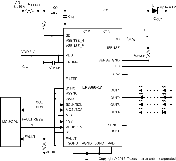 Figure 53. VDD = 5 V, I2C, 4 LED Outputs in Display Mode
9.2.1.1 Design Requirements
Table 24. EEPROM Setting Example
| ADDRESS (HEX) | DATA (HEX) |
|---|---|
| 60 61 62 63 64 65 66 67 68 69 6A 6B 6C 6D 6E 6F 70 71 72 73 74 75 76 77 78 |
ED DF DC F0 DF E5 F2 77 77 71 3F B7 17 EF B0 87 CE 72 E5 DF 35 06 DC FF 3E |
| DESIGN PARAMETER | VALUE |
|---|---|
| VIN voltage range | 3 V to 40 V |
| VDD voltage | 5 V |
| Charge pump | Disabled |
| Brightness Control | I2C |
| Output configuration | Mode 1, OUT1 to OUT4 are in display mode (phase shift 90º) |
| LED string current | 130 mA |
| External current set resistor | Disabled |
| Boost frequency | 303 kHz |
| Inductor | 22 μH to 33 μH, at least 9-A saturation current |
| Input/Output capacitors | 10 μF ceramic and 33 μF electrolytic |
| RISENSE | 20 mΩ |
| RSENSE | 25 mΩ |
| Current dimming with external NTC | Disabled |
9.2.1.2 Detailed Design Procedure
9.2.1.2.1 Inductor Selection
There are two main considerations when choosing an inductor; the inductor must not saturate, and the inductor current ripple must be small enough to achieve the desired output voltage ripple. Different saturation current rating specifications are followed by different manufacturers so attention must be given to details. Saturation current ratings are typically specified at 25°C. However, ratings at the maximum ambient temperature of application should be requested from the manufacturer. Shielded inductors radiate less noise and are preferable. The saturation current must be greater than the sum of the maximum load current and the worst case average-to-peak inductor current. The equation below shows the worst case conditions.
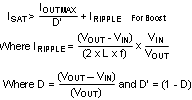
where
- IRIPPLE: peak inductor current
- IOUTMAX: maximum load current
- VIN: minimum input voltage in application
- L: min inductor value including worst case tolerances
- f: minimum switching frequency
- VOUT: output voltage
- D: Duty Cycle for CCM Operation
- VOUT: Output Voltage
As a result the inductor must be selected according to the ISAT. A more conservative and recommended approach is to choose an inductor that has a saturation current rating greater than the maximum switch current limit defined by <BOOST_IMAX_SEL[2:1]> EEPROM bits. A 22-µH to 33-µH inductor with a saturation current rating of at least 9 A is recommended for most applications. The inductor resistance must be less than 300 mΩ for good efficiency. See detailed information in Texas Instruments Application Note Understanding Boost Power Stages in Switch Mode Power Supplies (SLVA061). “Power Stage Designer™ Tools” can be used for the boost calculation: http://www.ti.com/tool/powerstage-designer.
9.2.1.2.2 Output Capacitor Selection
A ceramic capacitor with a 100-V voltage rating is recommended for the output capacitor. The DC-bias effect can reduce the effective capacitance by up to 80%, a consideration for capacitance value selection. Effectively the capacitance must be 33 µF for 600-mA loads. A different option is to use an aluminum electrolytic capacitor with low ESR and ceramic capacitor in parallel. Typically a 33-µF (ESR < 500 mΩ) with 10-µF (effective) ceramic capacitor in parallel is sufficient. If ESR is lower, capacitance for ceramic capacitor can be decreased.
For higher switching frequency (2.2 MHz) and boost output current below 400 mA, two 10-µF ceramic capacitors in parallel are sufficient.
9.2.1.2.3 Input Capacitor Selection
A ceramic capacitor with 50-V voltage rating is recommended for the input capacitor. The DC-bias effect can reduce the effective capacitance by up to 80%, a consideration for capacitance value selection. Effectively the capacitance must be 33 µF for 600-mA loads. A different option is to use an aluminum electrolytic capacitor with low ESR and ceramic capacitor in parallel. Typically a 33-µF (ESR < 500 mΩ) with 10-µF (effective) ceramic capacitor in parallel is sufficient. If ESR is lower, capacitance for ceramic capacitor can be decreased.
For higher switching frequency (2.2 MHz) and boost output current below 400 mA two 10-µF ceramic capacitors in parallel are sufficient.
9.2.1.2.4 Charge Pump Output Capacitor
A ceramic capacitor with at least 16-V voltage rating is recommended for the output capacitor of the charge pump. The DC-bias effect can reduce the effective capacitance by up to 80%, which needs to be considered in capacitance value selection. Typically a 10-µF capacitor is sufficient.
9.2.1.2.5 Charge Pump Flying Capacitor
A ceramic capacitor with at least 10-V voltage rating is recommended for the flying capacitor of the charge pump. Typically 1-µF capacitor is sufficient.
9.2.1.2.6 Diode
A Schottky diode must be used for the boost output diode. Peak repetitive current must be greater than inductor peak current (up to 9 A) to ensure reliable operation. Average current rating must be greater than the maximum output current. Schottky diodes with a low forward drop and fast switching speeds are ideal for increasing efficiency. Choose a reverse breakdown voltage of the Schottky diode significantly larger than the output voltage. Do not use ordinary rectifier diodes because slow switching speeds and long recovery times cause the efficiency and the load regulation to suffer.
9.2.1.2.7 Boost Converter Transistor
An nFET transistor with high enough voltage rating (VDS at least 5 V higher than maximum output voltage) must be used. Current rating for the FET must be the same as the inductor peak current. Gate-drive voltage for the FET is VDD or about 2 x VDD, if the charge pump is enabled (EEPROM selection).
9.2.1.2.8 Boost Sense Resistor
A high-power 25-mΩ resistor must be used for sensing the boost SW current. Power rating can be calculated from the inductor current and sense resistor resistance value.
9.2.1.2.9 Power Line Transistor
A pFET transistor with necessary voltage rating (VDS at least 5 V higher than max input voltage) must be used. Current rating for the FET must be the same as input peak current or greater. Transfer characteristic is very important for pFET. VGS for open transistor must be less then VIN. A 20-kΩ resistor between the pFET gate and source is sufficient.
If a pFET with high enough VDS and low VGS is not available, it is possible to use an nFET with extra external components with the EEPROM bit NMOS_PLFET_EN set high. See Charge Pump section (Figure 25) for using the nFET as a power-line FET.
9.2.1.2.10 Input Current Sense Resistor
A high-power 20-mΩ resistor must be used for sensing the boost input current. Power rating can be calculated from the input current and sense resistor resistance value.
9.2.1.2.11 Filter Component Values
Table 25 shows recommended filter component values for the VSYNC PLL filter (phase margin 60°). An external filter must be used only when external VSYNC is used; otherwise, the LP8860-Q1 uses internal compensation.
 Figure 54. Filter Components
Table 25. Filter Components Selection
| V/H SYNC | PLL FREQUENCY (MHz) | C1 | C2 | R1 |
|---|---|---|---|---|
| 50 Hz (BW3dB = 1 Hz) |
5 | 100 nF | 1.4 μF | 85 kΩ |
| 10 | 54 nF | 0.7 μF | 170 kΩ | |
| 20 | 27 nF | 0.35 μF | 338 kΩ | |
| 40 | 13.6 nF | 0.175 μF | 677 kΩ | |
| 20 kHz (BW3dB = 330 Hz) |
5 | 10 nF | 129 nF | 14 kΩ |
| 10 | 5 nF | 65 nF | 28 kΩ | |
| 20 | 2.5 nF | 32 nF | 56 kΩ | |
| 40 | 1.2 nF | 16 nF | 112 kΩ | |
| 50 kHz (BW3dB = 330 Hz) |
5 | 22 nF | 322 nF | 5.6 kΩ |
| 10 | 12 nF | 161 nF | 11.2 kΩ | |
| 20 | 6.2 nF | 80 nF | 22.3 kΩ | |
| 40 | 3.1 nF | 40 nF | 44,7 kΩ |
9.2.1.2.11.1 Critical Components for Design
Schematic on Figure 55 shows the critical part of circuitry: boost components, the LP8860-Q1 internal charge pump for gate driver powering and powering/grounding of LP8860-Q1 boost components. Layout example for this is shown in Figure 67.
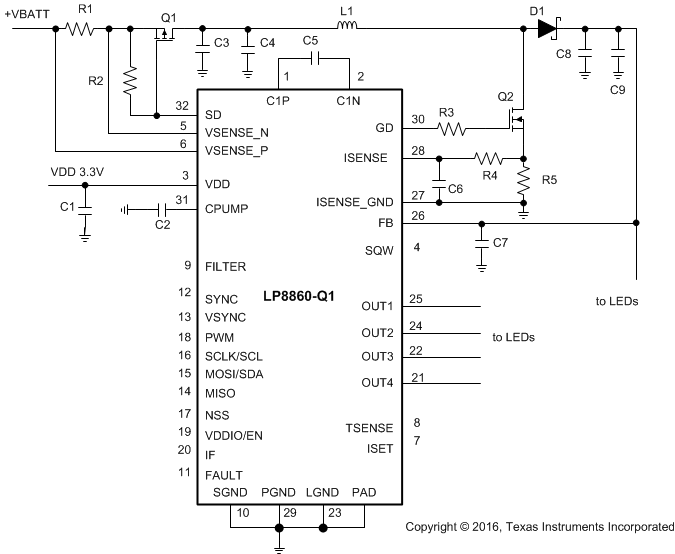 Figure 55. Critical Components for Design
Table 26. Bill of Materials for Design Example
| REFERENCE DESIGNATOR | DESCRIPTION | NOTE |
|---|---|---|
| R1 | 20 mΩ 3 W | Input current sensing resistor |
| R2 | 20 kΩ 0.1 W | Power-line FET gate pullup resistor |
| R3 | 10 Ω 0.1 W | Gate resistor for boost FET |
| R4 | 10 Ω 0.1 W | Current sensing filter resistor |
| R5 | 25 mΩ 3 W | Boost current sensing resistor |
| C1 | 1 μF 10 V ceramic capacitor | VDD bypass capacitor |
| C2 | 10 μF 16 V ceramic capacitor | Charge pump output capacitor |
| C3 | 33 μF 50 V electrolytic capacitor | Boost input capacitor |
| C4 | 10 μF 50 V ceramic capacitor | Boost input capacitor |
| C5 | 1 μF 10 V ceramic capacitor | Flying capacitor |
| C6 | 1000 pF 10 V ceramic capacitor | Current sensing filter capacitor |
| C7 | 39 pF 50 V ceramic capacitor | High frequency bypass capacitor |
| C8 | 33 μF 50 V electrolytic capacitor | Boost output capacitor |
| C9 | 10 μF 100 V ceramic capacitor | Boost output capacitor |
| L1 | 22 μH saturation current 9 A | Boost inductor |
| D1 | 60 V 15 A Schottky diode | Boost Schottky diode |
| Q1 | 60 V 10 A pMOSFET | Power-line FET |
| Q2 | 60 V 15 A nMOSFET | Boost nMOSFET |
9.2.1.3 Application Performance Plots
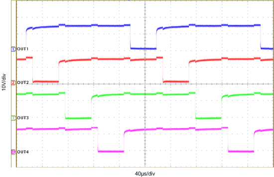
| fLED_PWM = 4.9 kHz | Phase shift 90º | 4 strings |
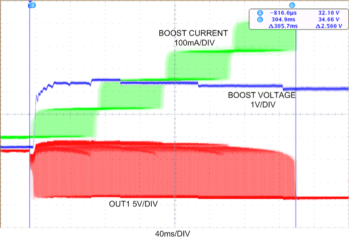
| PWM_SLOPE = 110 | 130 mA/string | Phase Shift = 90° |
| 4 strings | 10 LED/string | |
| EN_ADVANCED_SLOPE = 0 | ||
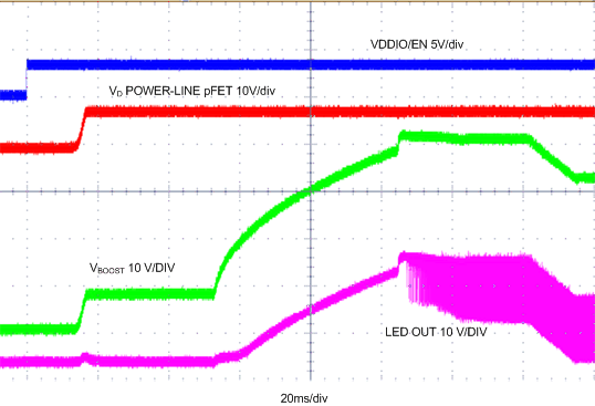
| ƒSW = 303 kHz | 130 mA/string |
| CIN = COUT= 33 µF(el) + 10 µF(cer) | |
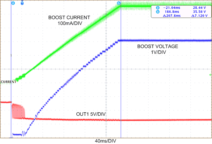
| EN_PWM_I = 1 | I_SLOPE =000 | 130 mA/string |
| PWM_SLOPE = 101 | GAIN_CTRL = 111 | 4 strings |
| EN_ADVANCED_SLOPE = 0 | Phase Shift = 90° | |
9.2.2 Low VDD Voltage and Combined Output Mode Application
Figure 60 shows the application for LED strings in Display mode (OUT1 and OUT2) and Cluster mode (OUT3 and OUT4). External powering must be used for Cluster-mode LED strings. VDD voltage is 3.3 V, and the charge pump for gate driver powering is enabled.
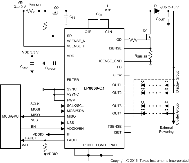 Figure 60. VDD = 3.3V, SPI, 2 Outputs in Display Mode,
 2 in Cluster Mode Schematic
9.2.2.1 Design Requirements
Table 27. EEPROM Setting Example
| ADDRESS (HEX) | DATA (HEX) |
|---|---|
| 60 61 62 63 64 65 66 67 68 69 6A 6B 6C 6D 6E 6F 70 71 72 73 74 75 76 77 78 |
ED DF DC F4 DF E5 F2 77 77 71 3F B7 17 EF B0 87 CF 72 E5 DF 35 06 DE FF 3E |
| DESIGN PARAMETER | VALUE |
|---|---|
| VIN voltage range | 3 V to 40 V |
| VDD voltage | 3.3 V |
| Charge pump | Enabled |
| Brightness Control | SPI |
| Output configuration | Mode 2, OUT1 and OUT2 - display mode (phase shift 180º), OUT3 and OUT4 - cluster mode |
| LED string current | OUT1 and OUT2 - 130 mA; OUT3 - 30 mA; OUT4 - 33 mA |
| External current set resistor | Disabled |
| Boost frequency | 303 kHz |
| Inductor | 22 μH to 33 μH, at least 5-A saturation current |
| Input/Output capacitors | 10 μF ceramic and 33 μF electrolytic |
| Current dimming with external NTC | Disabled |
9.2.2.2 Detailed Design Procedure
9.2.2.3 Application Performance Plots
9.2.3 High Output Voltage Application
The LP8860-Q1 has ability to control up to 16 or 17 LEDs per string with additional external components for output overvoltage protection. nFET transistors can protect outputs, and SQW output can be used to produce extra rail voltage for the transistor gates, if necessary voltage is not available in the system.
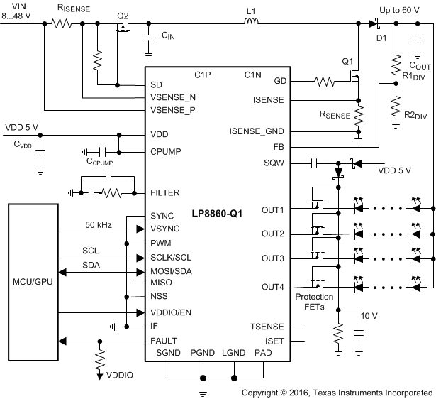 Figure 61. VDD = 5 V, I2C, High-Voltage Output with Output Protection FETs Circuits
9.2.3.1 Design Requirements
Table 28. EEPROM Setting Example
| ADDRESS (HEX) | DATA (HEX) |
|---|---|
| 60 61 62 63 64 65 66 67 68 69 6A 6B 6C 6D 6E 6F 70 71 72 73 74 75 76 77 78 |
ED DF DC F4 DF E5 F2 77 77 71 3F B7 17 EF B0 87 CF 72 E5 DF 35 06 DE FF 3E |
| DESIGN PARAMETER | VALUE |
|---|---|
| VIN voltage range | 3 V to 48 V |
| VDD voltage | 5 V |
| Charge pump | Disabled |
| Brightness Control | I2C |
| Output configuration | Mode 0, all outputs are in display mode, phase shift 90º, synchronized with VSYNC 50kHz, 10 LEDs per string, ƒLED_PWM= 10 kHz |
| LED string current | OUT1 to OUT4 - 120 mA |
| External current set resistor | Disabled |
| Boost frequency | 303 kHz |
| Inductor | 22 μH to 33 μH, at least 9-A saturation current |
| Input/Output capacitors | 10 μF ceramic and 33 μF electrolytic |
| Current dimming with external NTC | Disabled |
| VSYNC | Enabled, 50 kHz |
| Feedback voltage divider | R1DIV = 30 kΩ, R2DIV = 150 kΩ |
9.2.3.2 Detailed Design Procedure
9.2.3.3 Application Performance Plots
9.2.4 High Output Current Application
The LP8860-Q1 outputs can be tied together to drive LED with higher current. To drive a 300 mA/string, connect 2 outputs together. All 4 outputs connected together can drive up to a 600-mA LED string.
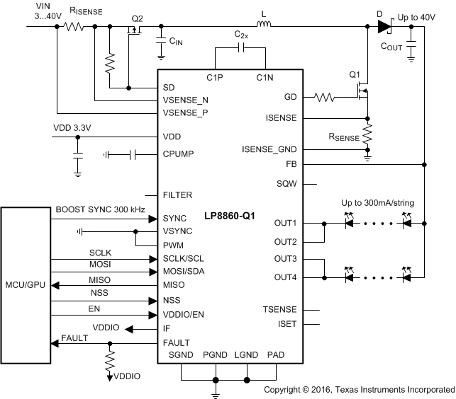 Figure 62. Two Channels at 300 mA/String, VDD = 3.3 V, SPI
9.2.4.1 Design Requirements
Table 29. EEPROM Setting Example
| ADDRESS (HEX) | DATA (HEX) |
|---|---|
| 60 61 62 63 64 65 66 67 68 69 6A 6B 6C 6D 6E 6F 70 71 72 73 74 75 76 77 78 |
EF FF DC F8 DF E5 F2 77 77 71 3F B7 17 EF B1 87 DF 72 E5 DF 35 06 DE FF 3E |
| DESIGN PARAMETER | VALUE |
|---|---|
| VIN voltage range | 3 V to 40 V |
| VDD voltage | 3.3 V |
| Charge pump | Enabled |
| Brightness Control | SPI |
| Output configuration | Mode 4, OUT1 to OUT4 in display mode, phase shift between tied groups 180º |
| LED string current | OUT1 and OUT2 - 300 mA; OUT3 and OUT4 - 300 mA |
| External current set resistor | Disabled |
| Boost frequency | 300 kHz externally synchronized |
| Inductor | 22 μH to 33 μH, at least 9-A saturation current |
| Input/Output capacitors | 10-μF ceramic and 33-μF electrolytic |
| Current dimming with external NTC | Disabled |
9.2.4.2 Detailed Design Procedure
9.2.4.3 Application Performance Plots
9.2.5 Three-Channel Configuration Without Serial Interface
Outputs which are not used can be left floating. In this example 3 outputs are in use. PSPWM mode for 3 outputs is set to mode 1 <LED_STRING_CONF[2:0]> = 001b, and the serial interface is not used. The device is enabled with the EN/VDDIO pin, and brightness control is set with the PWM input. EEPROM settings must be pre-programmed for brightness dimming with external PWM.
LED current dimming with external NTC sensor is used in this application to protect LEDs against over-heating.
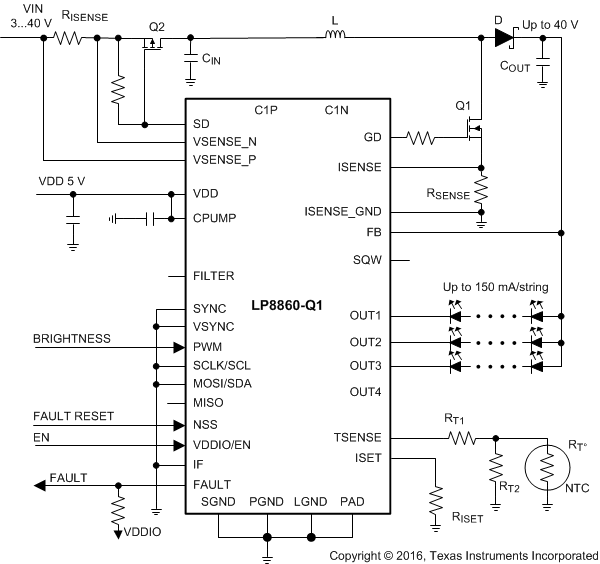 Figure 63. Three-Channel Configuration without Serial Interface
9.2.5.1 Design Requirements
Table 30. EEPROM Setting Example
| ADDRESS (HEX) | DATA (HEX) |
|---|---|
| 60 61 62 63 64 65 66 67 68 69 6A 6B 6C 6D 6E 6F 70 71 72 73 74 75 76 77 78 |
6F FF DC F2 DF E5 F8 77 77 E1 BF B7 17 EF B1 87 CE 72 E5 DF 35 06 DC CF 3F |
| DESIGN PARAMETER | VALUE |
|---|---|
| VIN voltage range | 3 V to 40 V |
| VDD voltage | 5 V |
| Charge pump | Disabled |
| Brightness Control | PWM |
| Output configuration | Mode 1, OUT1 to OUT3 - display mode; OUT4 - not used |
| LED string current | OUT1 to OUT3 - 150 mA |
| External current set resistor | Enabled, RISET = 24 kΩ |
| Boost frequency | 303 kHz |
| Inductor | 22 μH to 33 μH, at least 6-A saturation current |
| Input/Output capacitors | 10-μF ceramic and 33 μF electrolytic |
| Current dimming with external NTC | Enabled,RT°= NCP15XH103F03RC (Murata), see Figure 64, RT1 = 6.6 kΩ, RT2 not assembled |
9.2.5.2 Detailed Design Procedure
LED current dimming with external NTC sensor is used in this application — see section LED Current Dimming With External NTC Sensor for details. Figure 65 shows LED current de-rating versus temperature measured by NTC sensor with characteristic shown in Figure 64.
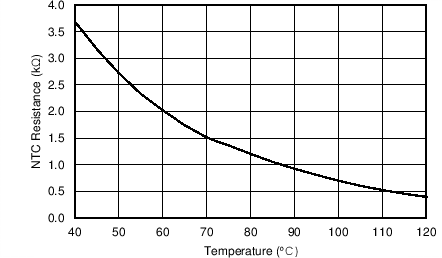 Figure 64. NTC Sensor Resistance vs Temperature
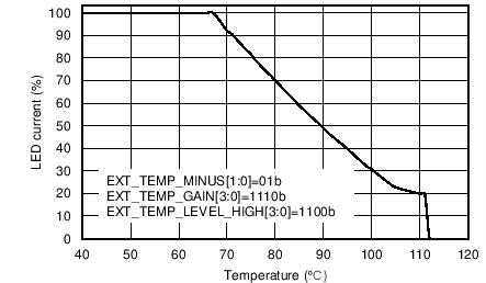 Figure 65. LED Current De-rating vs Temperature
9.2.5.3 Application Performance Plots
9.2.6 Solution With Minimum External Components
The LP8880-Q1 needs only a few external components for basic functionality if material cost and PCB area for a LP8860-Q1-based solution need to be minimized. In this example the power-line FET is removed, as is input current sensing. External synchronization functions are disabled.
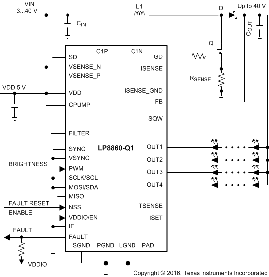 Figure 66. Solution With Minimum External Components
9.2.6.1 Design Requirements
Table 31. EEPROM Setting Example
| ADDRESS (HEX) | DATA (HEX) |
|---|---|
| 60 61 62 63 64 65 66 67 68 69 6A 6B 6C 6D 6E 6F 70 71 72 73 74 75 76 77 78 |
EF FF DC D0 DF E5 F0 77 77 71 3F B7 17 EF B0 87 CE 07 E5 DF 75 86 DC FF 3E |
| DESIGN PARAMETER | VALUE |
|---|---|
| VIN voltage range | 3 V to 40 V |
| VDD voltage | 5 V |
| Charge pump | Disabled |
| Brightness Control | PWM |
| Output configuration | Mode0, OUT1 to OUT4 in display mode, phase shift 90º |
| LED string current | OUT1 to OUT4 - 100 mA |
| External current set resistor | Disabled |
| Boost frequency | 2.2 MHz |
| Inductor | 4.7 µH to 22 µH, at least 6-A saturation current |
| Input/Output capacitors | 2 × 10-μF ceramic |
| Current dimming with external NTC | Disabled |