SNVSA50C August 2015 – May 2017 LP8861-Q1
PRODUCTION DATA.
- 1 Features
- 2 Applications
- 3 Description
- 4 Revision History
- 5 Device Comparison Table
- 6 Pin Configuration and Functions
-
7 Specifications
- 7.1 Absolute Maximum Ratings
- 7.2 ESD Ratings
- 7.3 Recommended Operating Conditions
- 7.4 Thermal Information
- 7.5 Electrical Characteristics
- 7.6 Internal LDO Electrical Characteristics
- 7.7 Protection Electrical Characteristics
- 7.8 Power Line FET Control Electrical Characteristics
- 7.9 Current Sinks Electrical Characteristics
- 7.10 PWM Brightness Control Electrical Characteristics
- 7.11 Boost/SEPIC Converter Characteristics
- 7.12 Logic Interface Characteristics
- 7.13 Typical Characteristics
-
8 Detailed Description
- 8.1 Overview
- 8.2 Functional Block Diagram
- 8.3 Feature Description
- 8.4 Device Functional Modes
-
9 Application and Implementation
- 9.1 Application Information
- 9.2 Typical Applications
- 10Power Supply Recommendations
- 11Layout
- 12Device and Documentation Support
- 13Mechanical, Packaging, and Orderable Information
Package Options
Mechanical Data (Package|Pins)
- PWP|20
Thermal pad, mechanical data (Package|Pins)
- PWP|20
Orderable Information
1 Features
- Qualified for Automotive Applications
- AECQ100 Qualified With the Following Results:
- Device Temperature Grade 1: –40°C to +125°C Ambient Operating Temperature
- Input Voltage Operating Range 4.5 V to 40 V
- Four High-Precision Current Sinks
- Integrated Boost/SEPIC Converter for LED String Power
- Power-Line FET Control for Inrush Current Protection and Standby Energy Saving
- Extensive Fault Detection and Tolerance Features
- Fault Output
- Input Voltage OVP, UVLO, and OCP
- Open and Shorted LED Fault Detection
- Automatic LED Current Reduction With External Temperature Sensor
- Thermal Shutdown
- Minimum Number of External Components
2 Applications
- Backlight for:
- Automotive Infotainment
- Automotive Instrument Clusters
- Smart Mirrors
- Heads-Up Displays (HUD)
- Central Information Displays (CID)
- Audio-Video Navigation (AVN)
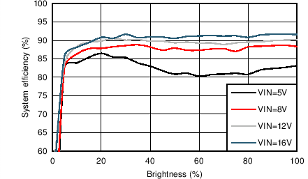
System Efficiency

3 Description
The LP8861-Q1 is an automotive high-efficiency, low-EMI, easy-to-use LED driver with integrated boost/SEPIC converter. It has four high-precision current sinks that can provide high dimming ratio brightness control with a PWM input signal.
The boost/SEPIC converter has adaptive output voltage control based on the LED current sink headroom voltages. This feature minimizes the power consumption by adjusting the voltage to lowest sufficient level in all conditions. The boost/SEPIC converter supports spread spectrum for switching frequency and an external synchronization with dedicated pin. A wide-range adjustable frequency allows the LP8861-Q1 to avoid disturbance for AM radio band.
The LP8861-Q1 has an option to drive an external p-FET to disconnect the input supply from the system in the event of a fault and reduce inrush current and standby power consumption. The device can reduce LED current based on temperature measured with external NTC sensor to protect LED from overheating and extend LED lifetime.
The input voltage range for the LP8861-Q1 is from 4.5 V to 40 V to support automotive stop/start and load dump condition. The LP8861-Q1 integrates extensive fault detection and protection features.
Device Information(1)
| PART NUMBER | PACKAGE | BODY SIZE (NOM) |
|---|---|---|
| LP8861-Q1 | TSSOP (20) | 6.50 mm × 4.50 mm |
- For all available packages, see the orderable addendum at the end of the data sheet.
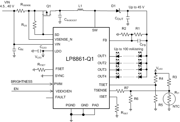
Simplified Schematic

4 Revision History
Changes from B Revision (April 2017) to C Revision
- Expanded descriptions for pins 3, 8, 9, 10, and 16 in Pin Functions Go
Changes from A Revision (November 2015) to B Revision
- Changed "Dimming Ratio of 10 000:1 at 200 Hz" to "Dimming Ratio of 10 000:1 at 100 Hz"Go
- Changed some minor wording of FeaturesGo
- Added new bulleted items to ApplicationsGo
- Changed "controller" to "converter" and "The high switching..." to "A wide-range adjustable..."Go
- Added Device Comparison Table tableGo
- Changed "In synchronization" to "If synchronization"Go
- Changes to PWM Brightness Control Electrical Characteristics: delete "IOUT = 100 mA. No external load from LDO" from Minimum ON/OFF time test conditions; move "0.5" from MAX to TYP in same row; add footnote 1Go
- Added footnote 1 to Boost/SEPIC Converter Characteristics for Toff, tsync_on_min, and tsync_off_minGo
- Deleted "Initial DC-DC voltage is about 88% of VMAX BOOST." from Integrated Boost/SEPIC Converter.Go
- Added definitions for Equation 1Go
- Added paragraph after Figure 9 Go
- Added new paragraph before Internal LDOGo
- Deleted "Dimming ratio is calculated as ratio between the input PWM period and minimum on/off time (0.5 μs)." from Brightness Control.Go
- Changed "less then" to "less than"Go
Changes from * Revision (August 2015) to A Revision
- Changed maximum Tstg from 160°C to 150°C Go
- Added last 2 sentences to end of Internal LDO.Go
- Changed Equation 3 Go
- Changed Figure 29 to update VIN and VSENSE_N pin connections; removed RISENSE row from sub-section 8.2.2.1 Design RequirementsGo